
Turnkey PCB Assembly is a complete manufacturing service in which one supplier manages design review, component sourcing, PCB fabrication, printed circuit board assembly, inspection, testing, and delivery of finished PCBA units. For engineers, the value is process ownership: the same manufacturing team checks Gerber data, BOM risk, centroid files, component availability, stencil design, SMT setup, reflow profile, through-hole integration, X-ray needs, ICT access, functional testing, and traceability before the circuit card assembly moves into production. IPC J-STD-001 defines soldering process and material requirements, while IPC-A-610 defines post-assembly acceptance criteria for electronic assemblies.
Learn more about: PCB Assembly Services for Engineers
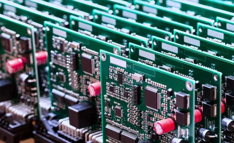
Turnkey PCB Assembly
What Turnkey Covers
Turnkey PCB Assembly connects fabrication, procurement, assembly, and testing under one controlled production workflow. Instead of sending bare boards to one supplier, parts to another, and test fixtures to a third, the turnkey supplier manages the complete build package.
A complete turnkey PCBA workflow usually covers:
- Gerber, ODB++, or IPC-2581 review
- Bill of Materials review
- Pick-and-place data review
- PCB fabrication
- Component sourcing
- Alternate part approval
- SMT stencil design
- Solder paste printing
- Component placement
- Reflow soldering
- Through-hole assembly
- AOI, X-ray, ICT, and functional test
- Firmware loading when required
- Labeling, packing, and delivery
PCB, PCBA, and Turnkey
| Term | Meaning | Turnkey Role |
|---|---|---|
| PCB | Bare printed circuit board | Fabricated before assembly |
| PCBA | PCB with soldered components | Main turnkey output |
| Circuit card assembly | Industrial term for assembled board | Used in controlled production records |
| Printed circuit assembly | Assembled electronic circuit board | Same practical meaning as PCBA |
| PCB manufacturing and assembly | Fabrication plus component assembly | Full turnkey responsibility |
IPC-2221 is a generic printed board design standard, and IPC-6012 defines qualification and performance requirements for rigid printed boards. These standards matter before assembly because fabrication quality affects final PCBA yield.
How It Works
Design Review
The turnkey process starts with engineering review. This step finds file errors, BOM risk, footprint mismatches, component shortages, soldering issues, and test access gaps before money is spent on boards and parts.
Design review checks:
- Gerber and drill alignment
- Board outline and slots
- Copper-to-edge clearance
- Solder mask openings
- Paste layer quality
- Component footprint match
- Polarity and orientation marks
- BGA, QFN, and fine-pitch package risk
- Test point access
- ICT fixture feasibility
- Conformal coating keepout
- IPC class requirement
| Review Item | Practical Check | Production Risk Reduced |
|---|---|---|
| Gerber package | Copper, mask, paste, silkscreen, outline | Missing or mismatched board layers |
| BOM | MPN, value, package, lifecycle | Wrong parts or unavailable parts |
| Centroid file | X/Y, rotation, side, refdes | Placement rotation errors |
| Footprints | Pad size, mask, paste, courtyard | Solder bridges and opens |
| Test access | Probe pads and fixture clearance | Low test coverage |
Sourcing
Component sourcing is one of the biggest reasons engineers choose turnkey PCBA. The supplier checks availability, pricing, MOQ, lead time, authenticity, packaging format, and substitute risk.
Sourcing controls:
- Match MPN exactly to BOM.
- Check lifecycle status: active, NRND, obsolete.
- Confirm packaging: reel, cut tape, tray, tube.
- Verify moisture sensitivity level for ICs.
- Approve alternate parts before purchasing.
- Avoid gray-market parts unless the customer authorizes them.
- Track date code and lot code for critical parts.
For high-reliability PCBA, sourcing is not just purchasing. It is risk control.
Fabrication
In full turnkey PCB fabrication and assembly, the same supplier or controlled partner fabricates the bare PCB before assembly. The board must match the assembly process.
Fabrication checks:
- Final board thickness: common values include 1.0 mm, 1.2 mm, 1.6 mm, and 2.0 mm
- Copper weight: 1 oz is common; 2 oz or higher for power boards
- Surface finish: ENIG, OSP, immersion silver, or HASL by project need
- Minimum trace and space: often 100/100 microns for standard designs
- Finished hole size: matched to THT lead diameter
- Controlled impedance: 50 ohm, 90 ohm, 100 ohm where required
- Electrical test: 100% E-test for production boards
Fabrication to Assembly
Assembly
Assembly converts the fabricated PCB into a functional PCBA. The exact route depends on SMT-only, THT-only, or mixed-technology requirements.
Core assembly sequence:
- Print solder paste through stencil.
- Inspect paste by SPI when required.
- Place SMT components.
- Reflow the first SMT side.
- Repeat for second side if needed.
- Insert through-hole components.
- Solder THT parts by wave, selective, or manual process.
- Inspect solder joints.
- Run electrical and functional tests.
- Pack and ship finished assemblies.
Core Process Parameters
| Process Step | Common Production Range | Why It Matters |
|---|---|---|
| Stencil thickness | 0.10-0.15 mm | Controls paste volume |
| Fine-pitch stencil | 0.08-0.10 mm by review | Supports QFN, BGA, 0201 |
| Placement accuracy | ±25-50 microns | Controls SMT alignment |
| Lead-free reflow peak | 235-250 C | Melts SAC solder alloy |
| Time above liquidus | 45-90 seconds | Forms solder joints |
| THT hole clearance | Lead diameter + 0.15-0.30 mm | Enables insertion and solder fill |
| Selective solder dwell | 2-5 seconds by joint mass | Controls wetting |
Testing and Delivery
Testing verifies that the PCBA works before delivery. The test plan should match the product risk, not only the order quantity.
Testing options:
- AOI for visible solder and placement
- X-ray for BGA, LGA, QFN, and hidden joints
- Flying probe for prototypes and low volume
- ICT for medium and high volume
- Boundary scan for dense digital boards
- Functional test for product behavior
- Thermal test for industrial and power products
- Firmware programming and serial number logging
IPC-A-610 is a post-assembly acceptance standard used to verify finished assemblies, while J-STD-001 focuses on soldering process and materials.
Learn more about: What Is PCB Assembly
Types of Turnkey Solutions
Full Turnkey
Full Turnkey means the supplier manages PCB fabrication, component sourcing, assembly, inspection, testing, and delivery.
Full turnkey is useful when:
- The project needs one manufacturing owner.
- Component sourcing is complex.
- Prototype schedule is tight.
- Engineering feedback must move quickly.
- The product uses BGA, QFN, fine-pitch ICs, or mixed THT.
- The buyer wants fewer supplier handoffs.
| Full Turnkey Item | Supplier Responsibility | Engineering Value |
|---|---|---|
| PCB fabrication | Board manufacturing and E-test | Fewer file transfer errors |
| Component sourcing | Purchase and AVL checking | Reduced procurement workload |
| SMT assembly | Paste, placement, reflow | Controlled solder process |
| THT integration | Insertion and soldering | Better mechanical reliability |
| Test | ICT or functional test | Ship-ready PCBA validation |
| Delivery | Packing and logistics | One accountable shipment |
Partial Turnkey
Partial Turnkey means the customer supplies some items, while the assembly supplier handles the rest. This model is common when engineers want to control expensive ICs, programmed parts, custom modules, or long-lead components.
Partial turnkey is useful when:
- The customer already owns inventory.
- Some parts require controlled programming.
- A critical chip has allocation risk.
- Engineering wants to approve key components.
- The supplier can source common passives and connectors.
Full Turnkey vs Partial Turnkey
| Item | Full Turnkey | Partial Turnkey |
|---|---|---|
| Component ownership | Supplier manages most or all parts | Customer supplies selected parts |
| Procurement workload | Lower for customer | Shared |
| Schedule risk | Supplier controls more variables | Customer kit delays can affect schedule |
| Best use | Fast prototype-to-production flow | Critical or allocated components |
| Accountability | More centralized | Split by supplied material |
| Main control point | AVL approval | Kit accuracy and incoming inspection |
Key Benefits
Faster Time-to-Market
Turnkey PCB Assembly reduces schedule loss caused by supplier handoffs. When the same team handles fabrication, sourcing, printed circuit assembly, and test, engineering questions move faster.
Time-saving examples:
- BOM risk is checked before purchasing.
- PCB fabrication notes are reviewed against assembly needs.
- Stencil design starts before all boards are completed.
- X-ray requirements are planned before BGA placement.
- Test fixture planning starts during prototype build.
- Failed pilot data returns to one process owner.
A practical prototype schedule can save several days when fabrication, SMT setup, and sourcing run in parallel instead of waiting in separate queues.
Simplified Supply Chain
Turnkey PCBA reduces purchasing and coordination work. It also reduces errors caused by incomplete handoffs.
Supply chain simplification includes:
- One purchase order
- One supplier communication path
- One DFM feedback loop
- One build schedule
- One quality report package
- One shipment of completed assemblies
This is especially valuable when a board contains 150 to 800 BOM lines, several package types, and multiple inspection requirements.
Lower Procurement Costs
Turnkey procurement can lower cost through consolidated purchasing, alternate part review, reel usage planning, and reduced freight between suppliers. The cost benefit depends on component availability and supplier purchasing strength.
Cost controls:
- Approve alternate parts early.
- Use standard resistor and capacitor values where possible.
- Avoid single-source components unless required.
- Allow reel planning for repeated builds.
- Separate prototype substitutions from production AVL.
- Review MOQ and attrition before purchase.
Fewer Errors
Turnkey reduces errors by connecting design review, sourcing, fabrication, assembly, and test. When one team owns the whole process, mismatches are easier to catch.
Typical errors reduced:
- Wrong package ordered from BOM
- Gerber and assembly drawing mismatch
- Centroid rotation mistake
- Incorrect stencil aperture
- Missing test pads
- BGA X-ray not planned
- THT keepout ignored
- Firmware not loaded before shipment
Quality Control
Turnkey QC Gates
A reliable turnkey process uses quality gates instead of one final check.
QC gates:
- File completeness review.
- BOM and AVL approval.
- Incoming component inspection.
- Bare PCB inspection.
- Stencil and paste review.
- First article inspection.
- AOI after reflow.
- X-ray for hidden solder joints.
- THT solder inspection.
- ICT or flying probe.
- Functional test.
- Final visual inspection.
- Packing and traceability check.
Documentation Records
Quality records give engineers proof that the build followed the agreed process.
Records may include:
- Approved BOM
- AVL and substitution log
- Material certificates
- Paste batch record
- Reflow profile
- AOI report
- X-ray images for BGA lots
- ICT report
- Functional test log
- Rework record
- Firmware version
- Serial number list
- Final inspection report
Getting Started
Files Needed
A turnkey build cannot start cleanly with Gerber files alone. The supplier needs design, sourcing, placement, assembly, and test data.
Required package:
- Gerber or ODB++ files
- Excellon drill file
- Board outline drawing
- Bill of Materials
- Pick-and-place centroid file
- Assembly drawing
- Fabrication drawing
- Approved vendor list
- Test procedure
- Firmware file if required
- Programming instructions
- Packaging instructions
- IPC class requirement
BOM Readiness
The BOM should be production-ready, not only design-readable.
A good BOM includes:
- Reference designator
- Quantity
- Manufacturer part number
- Approved alternates
- Description
- Value
- Tolerance
- Voltage or power rating
- Package
- Lifecycle status
- Customer-supplied status
- Do-not-populate marks
Centroid Data
The centroid file controls automated component placement. Rotation mismatch is one of the most common assembly problems in prototype builds.
Centroid data should include:
- Reference designator
- X coordinate
- Y coordinate
- Rotation
- Board side
- Package name
- Polarity note where needed
Before release, the centroid file should match the assembly drawing, BOM, and silkscreen orientation.
Two Key Comparisons
Turnkey vs In-House Coordination
| Item | Turnkey PCB Assembly | In-House Supplier Coordination |
|---|---|---|
| Supplier count | One main owner | Multiple suppliers |
| Schedule control | Centralized | Split between teams |
| BOM management | Supplier-supported | Customer-managed |
| Fabrication feedback | Linked to assembly | Often separated |
| Error responsibility | Easier to trace | Often disputed |
| Best fit | Fast builds and complex PCBA | Teams with mature supply chain |
Prototype Turnkey vs Production Turnkey
| Item | Prototype Turnkey | Production Turnkey |
|---|---|---|
| Build quantity | 1-100 boards | Hundreds to thousands |
| Main goal | Prove design and process | Repeatable yield and cost |
| BOM flexibility | Higher | Lower after AVL lock |
| Test method | Debug-friendly | Cycle-time-controlled |
| Inspection depth | Higher engineering review | Stable QC plan |
| Main output | Design correction data | Production baseline |
Real Factory Case
Project Background
A customer released a turnkey PCBA project for a compact industrial sensor gateway. The unit used a 6-layer PCB, one 0.5 mm BGA microcontroller, a wireless module, USB-C connector, two terminal blocks, a relay, LEDs, and a 24 V input power stage.
| Item | Project Data |
|---|---|
| Service model | Full turnkey PCB Assembly |
| Board type | Mixed SMT and THT PCBA |
| Layer count | 6 layers |
| Board thickness | 1.6 mm |
| Surface finish | ENIG |
| Smallest passive | 0201 |
| BGA pitch | 0.5 mm |
| THT parts | Relay, terminal blocks, shield tabs |
| Test method | ICT plus functional test |
| Thermal test | 40-minute run at 60 C |
Issue Found
The first 180-piece pilot build passed basic AOI, but full functional test exposed several issues:
- 6 boards reset during 24 V load switching.
- 5 boards had insufficient solder fill on relay pins.
- 4 boards showed wireless module startup failure after thermal soak.
- 3 boards had BGA void concentration above internal limit.
- First-pass yield was 90.0%.
Root causes:
- The BOM allowed two regulator alternates with different thermal pad layouts.
- The stencil aperture for the regulator pad was not adjusted for the selected alternate.
- Selective solder dwell time on the relay row was too short.
- BGA X-ray sampling was set at 15%, which missed early process drift.
- The functional test did not include fast 24 V load switching during the first run.
Corrective Result
The turnkey team locked one regulator MPN, reduced the thermal pad aperture by 18%, increased selective solder dwell from 2.8 seconds to 4.2 seconds, raised BGA X-ray inspection to 100% for the next pilot, and added load-switch cycling to the test procedure.
| Metric | First Pilot | Revised Pilot |
|---|---|---|
| Load-switch reset failures | 6/180 | 0/360 |
| Relay solder-fill defects | 5/180 | 0/360 |
| Wireless thermal failures | 4/180 | 1/360 |
| BGA void rejects | 3/180 | 1/360 |
| First-pass yield | 90.0% | 99.4% |
This case shows why turnkey PCBA is not only a buying model. It is an engineering feedback system that connects BOM control, stencil design, selective soldering, X-ray inspection, and functional testing.
Common Turnkey Errors
File Package Errors
- Missing centroid file
- BOM without approved manufacturer part numbers
- Assembly drawing missing polarity
- Gerber paste layer not reviewed
- Missing fabrication notes
- No IPC class requirement
- No firmware file or version control
- No packaging requirement
Sourcing Errors
- Unapproved part substitutions
- Obsolete parts left in BOM
- Wrong package ordered
- Cut-tape parts without attrition allowance
- Moisture-sensitive parts stored incorrectly
- Customer-supplied kits arriving short
- No AVL lock before pilot production
Assembly and Test Errors
- Reflow profile not measured on the actual board
- Stencil aperture copied from an older revision
- X-ray sampling too low for BGA pilot builds
- Selective solder keepout ignored
- ICT fixture started too late
- Functional test missing real load conditions
- Prototype rework not fed back into production notes
FAQ About Turnkey PCB Assembly
Question: What is Turnkey PCB Assembly?
Answer: Turnkey PCB Assembly is a manufacturing service where one supplier manages PCB fabrication, component sourcing, solder paste printing, component placement, reflow soldering, through-hole integration, inspection, testing, and delivery of finished PCBA units.
Question: What is the difference between full turnkey and partial turnkey?
Answer: Full turnkey means the supplier handles the PCB, components, assembly, testing, and delivery. Partial turnkey means the customer supplies selected components or materials while the supplier handles the remaining sourcing, assembly, inspection, and test work.
Question: What files are needed for turnkey PCBA?
Answer: A turnkey PCBA build needs Gerber or ODB++ files, drill files, BOM, centroid data, assembly drawing, fabrication drawing, approved vendor list, test procedure, firmware instructions when required, packaging instructions, and IPC class requirements.
Question: How should engineers choose turnkey PCB assembly?
Answer: Engineers should choose turnkey PCB assembly by checking the supplier’s fabrication control, component sourcing process, SMT capability, THT process, BGA X-ray capability, ICT or functional test support, traceability system, and ability to provide DFM feedback before the build starts.


![Understanding PCB Costs & Pricing [Your Complete Guide]](https://hdicircuitboard.com/wp-content/uploads/elementor/thumbs/Understanding-PCB-Costs-Pricing-Your-Complete-Guide-qzzhe6mcaxuolkux3xalfktgavumi9y1aqfbs9bpv4.webp "Understanding PCB Costs & Pricing [Your Complete Guide]")


