
8 and 14 Layer HDI PCBs with Stacked Vias: Comprehensive Design & Fabrication Guide
High Density Interconnect (HDI) PCBs with stacked vias have become foundational in miniaturized, high-performance electronics, with 8-layer and 14-layer configurations leading in applications from consumer devices to aerospace systems. These HDI circuit boards leverage stacked microvias to maximize routing density, reduce board size, and enhance signal integrity—addressing the core challenge of fitting complex circuitry into compact form factors. This guide details the technology, structure, stackups, manufacturing, and design solutions for 8-layer and 14-layer HDI PCBs with stacked vias, integrating industry standards and practical insights for hdi pcb manufacturer, supplier, and design teams.
Learn more about: How to Design HDI Microvia PCB
8-Layer HDI Technology with Stacked Vias
8-layer HDI PCBs with stacked vias strike a balance between density, performance, and cost, making them the most widely adopted configuration for mid-to-high complexity devices. They utilize sequential lamination and stacked microvias to enable high component density without compromising manufacturability—solving the dilemma of balancing functionality and production feasibility for hdi pcb fabrication.
Structure of 8-Layer HDI PCBs with Stacked Vias
The structure of 8-layer HDI PCBs with stacked vias is defined by sequential build-up (SBU) lamination and vertical interconnection via stacked microvias. Key structural elements include:
- Core Layers: A 4-layer core (typically layers 3-6) forms the backbone, providing mechanical stability. Core thickness ranges from 0.4mm to 0.6mm, using FR-4 or high-Tg materials (Tg ≥180°C) for thermal reliability.
- Build-Up Layers: Two build-up layers on each side of the core (layers 1-2 and 7-8) add routing density. Each build-up layer uses thin dielectrics (0.1mm-0.15mm) such as pre-preg or liquid epoxy.
- Stacked Vias: Laser-drilled microvias (diameter ≤6mil) stack vertically through build-up layers, connecting outer layers to the core. For example, vias from layer 1 stack to layer 2, then to layer 3 (core), creating a continuous vertical path.
- Annular Rings: Minimum annular ring of 2mil (0.05mm) per IPC-2221 Class 2 standards, ensuring reliable plating and mechanical strength for stacked vias.
Common Stackup for 8-Layer HDI PCBs with Stacked Vias
The most prevalent stackup for 8-layer HDI PCBs with stacked vias (often referenced as HDI PCB 2 n 2, indicating 2 build-up layers on each side of the core) follows this configuration (from top to bottom):
- Layer 1 (Top Signal): ½ oz copper, controlled-impedance routing for high-speed signals
- Layer 2 (Signal/Ground): ½ oz copper, adjacent to layer 1 for reference plane continuity
- Pre-preg (Build-Up Dielectric): 0.12mm, low-Dk material (Dk=3.4-3.8) for signal integrity
- Layer 3 (Core Signal/Power): 1 oz copper, part of the 4-layer core
- Layer 4 (Core Ground): 1 oz copper, solid reference plane for inner signals
- Core Dielectric: 0.5mm, FR-4 with Tg=180°C
- Layer 5 (Core Power): 1 oz copper, power distribution network (PDN) routing
- Layer 6 (Core Signal): 1 oz copper, part of the 4-layer core
- Pre-preg (Build-Up Dielectric): 0.12mm, matching top build-up layer
- Layer 7 (Signal/Ground): ½ oz copper, reference plane for bottom signal layer
- Layer 8 (Bottom Signal): ½ oz copper, component pad and signal routing
Total board thickness typically ranges from 0.8mm to 1.2mm, compatible with standard enclosure designs and PCB assembly processes.
Benefits of 8-Layer HDI PCBs with Stacked Vias
This configuration addresses key pain points in electronics design, delivering quantifiable advantages:
- Reduced Board Size: Stacked vias eliminate the need for large through-hole vias, reducing board area by 30-40% compared to standard 8-layer PCBs—critical for smartphones, wearables, and IoT devices.
- Enhanced Signal Integrity: Shortened signal paths via stacked vias reduce inductance and capacitance, lowering signal loss by 20-25% in high-speed (≥10Gbps) applications.
- Improved Thermal Management: Denser routing allows for strategic placement of thermal vias, improving heat dissipation by 15-20% compared to non-HDI 8-layer boards.
- Cost Efficiency: Balances density and fabrication complexity, with production costs 10-15% lower than 10-layer or 12-layer HDI configurations for similar functionality.
Applications of 8-Layer HDI PCBs with Stacked Vias
The versatility of 8-layer HDI PCBs with stacked vias makes them ideal for:
- Consumer Electronics: Smartphones, tablets, laptops, and wearables (e.g., smartwatches) where miniaturization is critical.
- Industrial Equipment: Programmable logic controllers (PLCs) and sensor modules requiring high component density and reliability.
- Medical Devices: Portable diagnostic tools and implantable devices (with biocompatible materials) where size and signal precision matter.
- Automotive Electronics: Advanced driver-assistance systems (ADAS) sensors and infotainment systems needing compact, robust circuitry.
Manufacturing Standards for 8-Layer HDI PCBs
Compliance with industry standards ensures consistency and reliability in hdi pcb fabrication:
- IPC-2226: Specifies HDI-specific design rules, including microvia dimensions (minimum diameter 4mil) and stacked via alignment tolerance (±0.002″).
- IPC-6012: Outlines performance requirements for rigid PCBs, including copper thickness (minimum 20µm for build-up layers) and dielectric integrity.
- IPC-4104: Governs base materials, requiring dielectrics with stable Dk and Df values to maintain signal integrity across temperature ranges.
- ISO 14644-1: Mandates Class 100 cleanroom conditions for laser drilling and lamination to prevent contamination of microvias.
14-Layer HDI PCBs with Stacked Vias
14-layer HDI PCBs with stacked vias cater to high-complexity applications requiring extreme density, multiple power domains, and robust signal integrity. They build on 8-layer technology with additional core and build-up layers, supporting advanced components like fine-pitch BGAs and high-speed interfaces—solving the challenge of integrating diverse functionalities in aerospace, defense, and enterprise electronics.
Technology of 14-Layer HDI PCBs with Stacked Vias
14-layer HDI PCBs utilize a hybrid lamination approach (sequential build-up + core lamination) and multi-tiered stacked vias to achieve high density. Key technological features include:
- Dual-Core or Thick Core Design: A 6-layer or 8-layer core (layers 4-11) provides mechanical rigidity, with thickness ranging from 0.6mm to 0.8mm. Some designs use dual 4-layer cores bonded with pre-preg for enhanced stability.
- Multi-Tier Build-Up Layers: 3 build-up layers on each side of the core (layers 1-3 and 12-14) enable ultra-dense routing. Thin dielectrics (0.08mm-0.12mm) are used to minimize total board thickness.
- Multi-Tier Stacked Vias: Stacked vias with 2-3 tiers connect outer build-up layers to the core. For example, vias from layer 1 stack to layer 2, then to layer 3, and finally to layer 4 (core), creating a vertical path through 3 build-up layers.
- Laser Drilling Precision: UV laser drilling for microvias ≤4mil, with positioning accuracy of ±0.001″ to ensure stacked via alignment across multiple layers.
Advantages of 14-Layer HDI PCBs with Stacked Vias
This configuration delivers critical benefits for high-complexity applications:
- Extreme Routing Density: Supports up to 50% more components per unit area than 8-layer HDI PCBs, enabling integration of multiple high-speed interfaces (e.g., PCIe 5.0, 5G) in a single board.
- Superior Signal Integrity: Isolated signal layers and dedicated reference planes reduce crosstalk by 30-35% compared to 8-layer designs, critical for RF PCBs and high-frequency applications.
- Multiple Power Domains: Dedicated power layers allow for 4-6 independent power domains, eliminating cross-contamination and improving power integrity for sensitive components.
- Enhanced Reliability: Sequential lamination reduces thermal stress during fabrication, with failure rates 25-30% lower than standard 14-layer through-hole PCBs in accelerated life tests.
Manufacturing of 14-Layer HDI PCBs
14-layer HDI PCB fabrication requires advanced processes and strict quality control to address complexity:
- Sequential Lamination: 4-5 lamination cycles (compared to 2-3 for 8-layer boards) to build up outer layers. Each cycle uses controlled temperature (180-200°C) and pressure (200-300 psi) to ensure dielectric bonding.
- Via Filling: Stacked vias filled with conductive or non-conductive epoxy to prevent voids and ensure planarity. Conductive filling is used for power vias to enhance current-carrying capacity.
- Plating Control: Electroless copper plating (0.5-1µm) followed by electrolytic copper plating (20-25µm) to ensure uniform coverage in microvias, with thickness variation ≤10% per IPC-6012 Class 3.
- Inspection & Testing: X-ray inspection for stacked via alignment, AOI (Automated Optical Inspection) for trace defects, and TDR (Time Domain Reflectometry) for impedance verification.
Design Considerations for 14-Layer HDI PCBs
Design teams must address unique challenges to ensure manufacturability and performance:
- Layer Stackup Optimization: Symmetrical stackup (e.g., signal-ground-signal-power-power-signal-ground-signal) to prevent board warpage. Dedicated reference planes for each signal layer to maintain return path continuity.
- Via Placement: Stacked vias placed in non-critical areas to avoid overlapping with component pads. Minimum spacing of 10mil between stacked via clusters to prevent dielectric weakening.
- Impedance Control: Tight impedance tolerance (±3%) for high-speed signals, achieved through precise trace width (3-5mil) and dielectric thickness (0.1mm) control.
- Thermal Management: Thermal vias (10-12mil diameter) placed near high-power components (e.g., BGAs, voltage regulators) to dissipate heat. Thermal pads with 50% via coverage for components with power dissipation ≥2W.
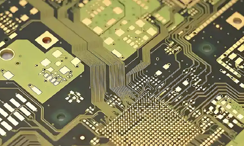
Via Technology in 8 & 14 Layer HDI PCBs
Via technology is the backbone of HDI PCBs, with stacked vias enabling the density and performance that distinguish these boards from standard configurations.
Stacked Vias vs. Staggered Vias
| Characteristic | Stacked Vias | Staggered Vias |
|---|---|---|
| Routing Density | 30-40% higher | Lower (requires more horizontal space) |
| Manufacturing Complexity | Higher (requires precise alignment) | Lower (more forgiving of misalignment) |
| Signal Integrity | Better (shorter signal paths) | Slightly reduced (longer paths) |
| Cost | 15-20% higher | Lower (fewer lamination cycles) |
| Use Case | 8-layer/14-layer HDI PCBs with fine-pitch BGAs | Less dense HDI designs or cost-sensitive projects |
Microvias in Stacked Configurations
Microvias (diameter ≤6mil) are the foundation of stacked via technology, with key specifications:
- Aspect Ratio: Maximum 0.75:1 (depth-to-diameter) to ensure reliable plating, per IPC-2226.
- Materials Compatibility: Laser-drilled microvias work with low-Dk dielectrics (e.g., Rogers 4350, Isola I-Speed) to minimize signal loss.
- Current-Carrying Capacity: 0.8-1.2A per microvia (6mil diameter, 1oz copper plating) for power routing.
Via-in-Pad Technology
Via-in-Pad (VIP) integrates vias directly within component pads, critical for fine-pitch BGAs (≤0.5mm pitch) in 8-layer and 14-layer HDI PCBs:
- Filling Requirements: VIPs filled with epoxy and plated over to maintain planarity, preventing solder wicking during assembly.
- Performance Benefits: Reduces trace length by 25-30% compared to dogbone routing, lowering inductance and improving signal integrity.
- Manufacturing Specifications: Pad size 20-30% larger than microvia diameter, with minimum copper wrap of 5mil per IPC-6016.
Layer Stackup & Thickness for 8/14 Layer HDI PCBs
Layer stackup directly impacts performance, manufacturability, and cost, with thickness optimized for specific applications.
Thickness Specifications
| Configuration | Total Thickness Range | Core Thickness | Build-Up Layer Thickness (Per Side) |
|---|---|---|---|
| 8-Layer HDI | 0.8mm-1.2mm | 0.4mm-0.6mm | 0.2mm-0.3mm (2 layers) |
| 14-Layer HDI | 1.2mm-1.6mm | 0.6mm-0.8mm | 0.3mm-0.4mm (3 layers) |
Stackup Optimization for Signal Integrity
- Reference Plane Continuity: Solid ground/power planes adjacent to signal layers to stabilize impedance and provide low-inductance return paths.
- Dielectric Selection: Low-Dk (3.0-3.8) and low-Df (≤0.005) materials for build-up layers to minimize signal attenuation in high-speed applications.
- Power Plane Placement: Power planes placed between ground planes to increase interplane capacitance, reducing PDN noise by 20-25%.
Manufacturing Complexities & Cost Management
8-layer and 14-layer HDI PCBs with stacked vias present unique manufacturing challenges, with cost management strategies tailored to balance performance and budget.
Key Manufacturing Complexities
- Lamination Alignment: Tolerance of ±0.002″ for sequential lamination to ensure stacked via alignment, requiring advanced registration equipment.
- Microvia Drilling: UV laser drilling for small diameters (≤4mil) with high precision, increasing fabrication time by 20-30% compared to standard drilling.
- Via Filling: Epoxy filling of stacked vias to prevent voids, adding 1-2 manufacturing steps and increasing labor costs.
Cost Management Strategies
- Optimize Layer Count: Use 8-layer HDI for mid-complexity designs instead of 10-layer to reduce lamination cycles and material costs.
- Standardize Via Sizes: Limit stacked via diameters to 2-3 sizes to streamline drilling and filling processes, reducing setup time by 15-20%.
- Material Selection: Balance performance and cost by using FR-4 for core layers and low-Dk materials only for high-speed signal layers.
- Volume Optimization: Batch production to leverage economies of scale, reducing per-unit costs by 10-15% for orders ≥1000 units.
HDI PCB Routing Common Solutions
Routing dense 8-layer and 14-layer HDI PCBs requires specialized strategies to maximize density and maintain signal integrity.
H3: Use Microvias for Fanout
- Fine-Pitch BGA Fanout: Microvias enable fanout of 0.4mm-0.5mm pitch BGAs, supporting 2-3 traces per pin row compared to 1 trace with through-hole vias.
- Escape Routing: Stacked microvias route signals from inner BGA rows to outer layers, reducing congestion by 30-40% in critical areas.
Proper Stack-Up Management
- Signal Layer Grouping: Group high-speed signals (e.g., PCIe, DDR) on dedicated layers with adjacent reference planes to minimize crosstalk.
- Power Domain Isolation: Separate analog and digital power planes to prevent noise coupling, with minimum spacing of 20mil between domains.
Design for Manufacturability (DFM)
- Trace Width/Spacing: Minimum 3mil/3mil for inner layers and 4mil/4mil for outer layers, per IPC-2221, to ensure reliable etching.
- Annular Ring: Minimum 2mil annular ring for microvias to prevent drill breakout, a common cause of manufacturing defects.
- Test Points: Incorporate test points on outer layers for flying probe testing, with minimum size of 30mil to ensure accessibility.
Rigorous DRC (Design Rule Check)
- Pre-Fabrication DRC: Validate against manufacturer-specific rules for microvia size, spacing, and stackup alignment.
- Signal Integrity DRC: Check for impedance mismatches, crosstalk, and signal reflections using CAD tools with field solvers.
- Manufacturing DRC: Verify compliance with IPC standards for copper thickness, dielectric integrity, and via filling.
FAQ: 8/14 Layer HDI PCBs with Stacked Vias
What is the difference between HDI PCB 2 n 2 and standard HDI configurations?
HDI PCB 2 n 2 refers to 2 build-up layers on each side of an n-layer core (e.g., 8-layer HDI = 2+4+2), optimizing density for mid-complexity designs. Standard HDI may have 1 or 3 build-up layers, with 2 n 2 striking a balance between density and cost.
How to choose between 8-layer and 14-layer HDI PCBs?
Select 8-layer HDI for designs with ≤500 components, 0.5mm pitch BGAs, and moderate speed requirements (≤10Gbps). Choose 14-layer HDI for ≥1000 components, fine-pitch BGAs (≤0.4mm), multiple high-speed interfaces, and extreme density needs.
What IPC standards are critical for HDI PCB fabrication?
Key standards include IPC-2226 (HDI design rules), IPC-6012 (performance requirements), IPC-4104 (materials), and IPC-6016 (HDI-specific qualification), ensuring consistency and reliability across manufacturers.
Can flexible printed circuit or rigid flex pcb use 8/14 layer HDI with stacked vias?
Yes—flexible printed circuit and rigid flex pcb configurations support 8-layer HDI (with thinner dielectrics: 0.05mm-0.08mm) for compact, flexible electronics. 14-layer HDI is less common for flexible designs due to thickness constraints but used in rigid-flex hybrid systems for aerospace applications.
What is the typical lead time for hdi pcb fabrication of 8/14 layer boards?
Lead time ranges from 2-3 weeks for 8-layer HDI (prototypes) and 3-4 weeks for 14-layer HDI, with volume production (≥1000 units) adding 1-2 weeks due to additional quality control steps.
Conclusion
8-layer and 14-layer HDI PCBs with stacked vias represent the gold standard for high-density, high-performance electronics, enabling miniaturization and advanced functionality in consumer, industrial, medical, and aerospace applications. By leveraging stacked vias, optimized layer stackups, and strict adherence to IPC standards, these HDI circuit boards solve the core challenge of fitting complex circuitry into compact form factors while maintaining signal integrity and reliability. Whether working with a hdi pcb manufacturer, supplier, or in-house design team, understanding the technology, manufacturing requirements, and design solutions outlined in this guide ensures successful implementation of 8-layer and 14-layer HDI PCBs with stacked vias.


![Understanding PCB Costs & Pricing [Your Complete Guide]](https://hdicircuitboard.com/wp-content/uploads/elementor/thumbs/Understanding-PCB-Costs-Pricing-Your-Complete-Guide-qzzhe6mcaxuolkux3xalfktgavumi9y1aqfbs9bpv4.webp "Understanding PCB Costs & Pricing [Your Complete Guide]")


