
Via-in-Pad HDI PCB design places a via directly inside a component pad to save routing space, shorten signal paths, improve thermal transfer, and support fine-pitch BGA or QFN breakout. A reliable Via-in-Pad structure is not only a drilled hole in a pad. It needs controlled drilling, plating, filling, capping, planarization, annular ring, aspect ratio, stack-up design, solderability, and inspection. For engineers, Via-in-Pad becomes valuable when standard dogbone fanout cannot meet density, but it also raises hdi pcb fabrication cost and assembly risk if VIPPO quality is not defined before layout release.
Via-in-Pad Basics
Via-in-Pad Function
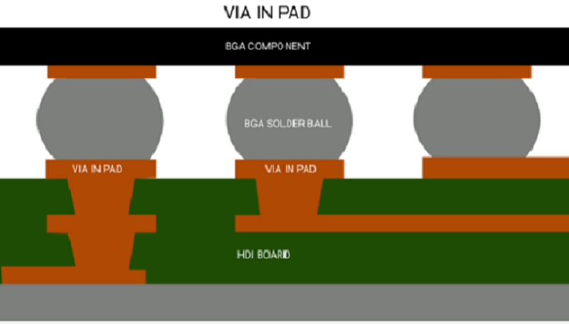
Via-in-Pad, often shortened as VIP, means a via is placed inside the solderable pad of a component instead of beside the pad. In high density interconnect designs, this structure gives dense components direct access to inner signal, power, or ground layers.
Common VIP applications include:
- 0.5 mm and 0.4 mm BGA fanout
- Fine-pitch QFN and LGA packages
- Processor, FPGA, memory, and AI module breakout
- Short decoupling capacitor loops
- RF ground transitions
- High-current thermal pads
- Compact wearable and medical electronics
- Miniaturized industrial controller modules
IPC-2221 provides generic printed board design requirements, while IPC-2226 is the sectional design standard used for HDI structures and microvia design. IPC-6012 defines qualification and performance requirements for rigid printed boards, including multilayer boards with blind and buried vias.
VIP vs Dogbone Fanout
| Item | Conventional Dogbone Fanout | Via-in-Pad HDI |
|---|---|---|
| Via location | Outside component pad | Inside component pad |
| Best pitch range | 0.8 mm and larger | 0.5 mm and smaller |
| Routing density | Medium | High |
| Signal path | Longer | Shorter |
| Assembly risk | Lower if spacing exists | Requires fill and cap control |
| Process cost | Lower | Higher |
| Inspection need | Standard AOI and E-test | X-ray, microsection, planarity check |
Dogbone fanout remains the lower-cost option when the package pitch and board outline allow it. Via-in-Pad should be used when density, electrical path length, thermal transfer, or board size makes conventional fanout impractical.
Why Use Via-in-Pad
Space Optimization
Space optimization is the main reason engineers choose Via-in-Pad. A fine-pitch BGA may not have enough room for a via land, trace, clearance, and solder mask bridge between adjacent balls. Placing the via inside the pad removes the dogbone structure and sends the connection directly into the stack-up.
VIP supports space reduction by:
- Removing lateral fanout around dense packages
- Opening more surface routing channels
- Reducing breakout distance from inner BGA rows
- Allowing tighter component placement
- Preserving area for decoupling capacitors
- Reducing total board outline in compact products
- Supporting thinner and smaller hdi circuit boards
Signal Integrity
Signal integrity improves when Via-in-Pad shortens the transition from the component pad to the target routing layer. This is useful for interfaces where discontinuity, stub length, return path, and impedance control matter.
Typical controlled impedance targets include:
| Signal Type | Typical Target | VIP Design Value |
|---|---|---|
| Single-ended clock | 50 ohm | Shorter transition and cleaner reference return |
| USB differential | 90 ohm | Reduced breakout detour |
| Ethernet / LVDS | 100 ohm | Better pair escape from dense packages |
| PCIe differential | 85 ohm | Lower via stub and shorter layer change |
| RF control | 50 ohm | Short ground return and reduced loop area |
Via-in-Pad does not automatically solve signal integrity. It must be paired with continuous reference planes, controlled dielectric thickness, copper roughness review, impedance coupons, and proper ground stitching near layer transitions.
Thermal Management
Thermal management is another reason to use VIP. Power ICs, QFN packages, RF devices, LED drivers, and BGA processors often need heat to move from the package pad into inner copper planes.
| Thermal Use Case | VIP Role | Process Control |
|---|---|---|
| QFN exposed pad | Transfers heat into internal planes | Filled and capped vias |
| Power regulator | Reduces local temperature rise | Copper balance and via array |
| RF amplifier | Improves ground and thermal path | Low-loss material and ground via pattern |
| LED driver | Spreads heat into copper area | Copper weight and void control |
| BGA processor | Supports power and ground fanout | X-ray and reflow validation |
Open vias inside thermal pads can pull solder away during reflow. For solderable pads, VIPPO is usually required to prevent solder wicking and void formation.
VIPPO Process
Why VIPPO Matters
VIPPO means via-in-pad plated over. The via is drilled, plated, filled, capped, and planarized to create a flat solderable surface. Without VIPPO, solder can flow into the via during reflow. That creates insufficient solder volume, BGA voiding, tilted QFN packages, weak joints, and hidden assembly failures.
VIPPO controls:
- Solder wicking into via cavities
- BGA ball collapse variation
- QFN pad floating
- Local solder voids
- Exposed fill material
- Pad dimple or protrusion
- Hidden reliability defects
VIPPO Process Steps
| Process Step | Factory Operation | Key Control |
|---|---|---|
| Drilling | Laser or mechanical via formation | Diameter, depth, debris, target pad condition |
| Plating | Copper deposition in via wall | Continuity, copper thickness, adhesion |
| Filling | Resin, conductive, or copper fill | Void-free fill and thermal behavior |
| Capping | Copper cap over filled via | Closed solderable surface |
| Planarization | Surface leveling before finish | Dimple, protrusion, pad flatness |
| Surface finish | ENIG, ENEPIG, OSP, or other finish | Solderability and planarity |
| Inspection | X-ray, microsection, visual checks | Fill voids, cap cracks, dimple control |
Drilling
Drilling method depends on via size, depth, pad size, and layer connection. Fine-pitch HDI designs usually use laser microvias because laser drilling supports small diameters and short layer-to-layer transitions.
Practical drilling values:
- Laser microvia diameter: 75-125 microns
- Advanced laser microvia: 50-75 microns by review
- Mechanical via-in-pad: 0.15-0.30 mm by review
- Build-up dielectric thickness: 50-80 microns common
- Microvia depth: no more than 0.25 mm under IPC-style definition
- Microvia aspect ratio: maximum 1:1
Current IPC-related descriptions define a microvia as a blind structure with a maximum 1:1 aspect ratio and total depth no more than 0.25 mm from capture land to target land.
Plating
Plating creates the conductive path from the pad to the target layer. In VIP structures, plating quality affects both electrical continuity and mechanical reliability.
Plating controls include:
- Via wall copper thickness
- Target pad adhesion
- Electroless copper activation
- Electroplating uniformity
- Void-free copper deposition
- Copper cap bonding
- Microsection sampling
- Thermal stress validation
A plated via may pass bare-board E-test but still crack after reflow or thermal cycling if the copper is thin or poorly bonded.
Filling
Filling prevents solder from entering the via and supports the cap surface. The filling method must match electrical, thermal, and assembly requirements.
| Fill Type | Best Use | Main Tradeoff |
|---|---|---|
| Nonconductive epoxy fill | General VIPPO under BGA and QFN | Stable assembly, lower thermal transfer |
| Conductive fill | Ground or thermal paths | Better conductivity, more process-sensitive |
| Copper fill | Stacked microvias and high-density HDI | Strong thermal and electrical path, higher cost |
| Resin plug plus cap | Standard solderable VIP | Good planarity after controlled process |
| Open via | Non-solderable areas only | High solder wicking risk in pads |
For solderable pads, open via-in-pad should be avoided because the assembly defect often appears after the bare hdi pcb has already passed electrical testing.
Capping and Planarization
Capping and planarization decide whether the finished pad behaves like a normal component pad. A via that is filled but not flat can still create solder imbalance.
| VIPPO Quality Item | Practical Target | Defect Controlled |
|---|---|---|
| Dimple after planarization | Below 10-15 microns | Uneven solder volume |
| Copper cap coverage | Continuous cap, no exposed fill | Poor solderability |
| Protrusion | Controlled below pad flatness limit | Component tilt |
| Fill void | Not allowed in critical VIP | Hidden reliability failure |
| Surface finish | ENIG or ENEPIG for fine pitch | Stable soldering surface |
For 0.4 mm and 0.5 mm BGA packages, small pad height differences can change ball collapse and X-ray appearance across the package.
Design Guidelines
Aspect Ratio
Aspect ratio is via depth divided by via diameter. For laser microvias, a 1:1 ratio is a maximum limit, not the best production target. Many production teams prefer 0.75:1 or lower when reliability matters.
| Via Depth | Via Diameter | Aspect Ratio | Design Judgment |
|---|---|---|---|
| 50 microns | 100 microns | 0.50:1 | Strong margin |
| 60 microns | 90 microns | 0.67:1 | Good production range |
| 75 microns | 100 microns | 0.75:1 | Reliable HDI target |
| 80 microns | 80 microns | 1.00:1 | Upper boundary |
| 90 microns | 75 microns | 1.20:1 | Avoid for standard microvia |
Aspect ratio should be locked with the stack-up. A dielectric change after layout can convert a safe VIP design into a high-risk fabrication feature.
Microvia Limitations
Microvia limitations come from drilling, plating, dielectric thickness, lamination cycles, and thermal stress.
Main limitations:
- Smaller vias are harder to plate consistently.
- Thick dielectric increases aspect ratio.
- Stacked microvias need copper filling.
- Repeated lamination creates registration movement.
- Fine-pitch BGA needs very tight pad flatness.
- Ultra-small capture pads reduce annular ring margin.
- High-current pads may need multiple filled vias or copper-filled structures.
Annular Ring
Annular ring is the copper land remaining around a drilled or laser-drilled via. Even in Via-in-Pad designs, annular ring matters because registration movement can reduce the effective land around the via.
| Design Item | Conservative Target | Dense HDI Target |
|---|---|---|
| Annular ring | 75 microns | 50 microns by review |
| Capture pad oversize | Via diameter + 100-150 microns | Via diameter + 75-100 microns |
| Target pad oversize | Via diameter + 80-120 microns | Via diameter + 60-90 microns |
| Plane clearance | 200-300 microns | 150-250 microns by review |
Tight annular ring values should be approved by the hdi pcb manufacturer before routing. CAD clearance alone does not prove fabricability.
Manufacturer Alignment
Manufacturer alignment means the design rules, stack-up, drawings, and inspection criteria match the actual factory process.
Before layout release, engineers should confirm:
- Minimum laser via diameter
- Maximum microvia depth
- Preferred aspect ratio
- Capture pad and target pad size
- VIP fill material
- Copper cap requirement
- Dimple limit after planarization
- Surface finish compatibility
- Stacked vs staggered microvia policy
- X-ray and microsection plan
- Controlled impedance coupon design
- IPC class and acceptance criteria
Manufacturing Guidelines
Stack-Up Co-design
Via-in-Pad should be designed with the stack-up, not added after routing congestion appears. The stack-up decides dielectric thickness, target layer, copper thickness, and lamination sequence.
Stack-up data should include:
- Total layer count
- HDI type: 1+N+1, 2+N+2, 3+N+3, or any-layer
- VIP start and target layers
- Microvia layer pairs
- Buried via layer pairs
- Through via rules
- Buildup dielectric thickness
- Copper weight by layer
- Controlled impedance layers
- Surface finish
- Final board thickness
Stacked vs Staggered VIP
| Item | Staggered VIP Microvias | Stacked VIP Microvias |
|---|---|---|
| Routing density | High | Highest |
| Cost | Lower | Higher |
| Copper fill requirement | Lower in many cases | Required |
| Reliability margin | Better when space allows | Process-dependent |
| Best use | 0.5 mm BGA with available offset | 0.4 mm BGA or extreme density |
| Inspection | Microsection sampling | X-ray and strict microsection |
Staggered structures should be used when routing space allows. Stacked structures are valuable when vertical density is required, but they need stronger filling and inspection control.
Surface Finish Choice
| Surface Finish | VIP Use | Engineering Note |
|---|---|---|
| ENIG | Fine-pitch BGA and QFN | Flat surface, common for VIPPO |
| ENEPIG | Wire bonding or high-reliability mixed assembly | More versatile, higher cost |
| OSP | Cost-sensitive SMT | Flat but shorter shelf-life control |
| Immersion silver | High-speed and RF designs | Handling and tarnish control needed |
| HASL | Not ideal for fine-pitch VIP | Planarity risk |
ENIG is widely used for fine-pitch Via-in-Pad HDI because pad flatness and solderability matter more than small finish-cost savings.
Two Key Comparisons
Filled VIP vs Tented Via
| Item | Filled VIPPO | Tented Via |
|---|---|---|
| Location | Inside solder pad | Usually outside solder pad |
| Assembly use | Suitable for solderable pads | Not reliable for solderable pads |
| Solder wicking control | Strong | Weak if via is in pad |
| Cost | Higher | Lower |
| Inspection | X-ray and microsection | Visual and AOI |
| Best use | BGA, QFN, dense HDI | Non-pad via protection |
A tented via is not a replacement for VIPPO when the via sits inside a solderable pad.
VIP vs Through-Hole Fanout
| Item | Via-in-Pad HDI | Through-Hole Fanout |
|---|---|---|
| Routing space | Saves surface area | Consumes more routing channels |
| Via stub | Short or minimized | Full board-height stub |
| Best package pitch | 0.5 mm and below | 0.8 mm and larger |
| Cost | Higher | Lower |
| Fabrication complexity | Fill, cap, planarization | Standard drilling and plating |
| Best use | Compact high density interconnect boards | Lower-density products |
Quality Control Plan
Bare Board Inspection
Via-in-Pad HDI quality control should be defined before quote and panel design.
Required inspection items:
- CAM and DFM review
- Stack-up verification
- Laser drilling inspection
- Desmear and cleaning control
- Copper plating thickness check
- Via fill void inspection
- Copper cap continuity check
- Planarity and dimple measurement
- X-ray for filled or stacked vias
- Microsection coupons near critical VIP areas
- 100% electrical test
- Impedance coupon testing
- Solder mask registration review
- Warpage check after thermal simulation
Assembly-Level Validation
VIP defects often appear at the assembled-board level because the solder joint is affected by pad flatness and fill quality.
Assembly validation should include:
- Solder paste inspection
- Reflow profile validation
- BGA or QFN X-ray
- Void review over VIP areas
- Functional test under load
- Thermal soak for high-density products
- Rework limit definition
- Failure analysis loop from PCBA back to PCB process
PCB is the bare printed circuit board. PCA is the assembled board with components, solder joints, labels, firmware, inspection records, and functional test data. A VIP board can pass PCB E-test while the PCA fails because of solder wicking, voiding, poor collapse, or thermal instability.
Real Factory Case
Project Background
A compact AI sensor module used a 0.4 mm BGA processor, LPDDR memory, MIPI camera input, USB, PMIC, flash, and a board-to-board connector. The first layout used dogbone fanout around the processor, but the inner BGA rows forced long detours and blocked decoupling placement.
| Item | Original Design | VIP HDI Revision |
|---|---|---|
| Board type | Standard multilayer concept | Via-in-Pad HDI PCB |
| Layer count | 8 layers | 10 layers |
| HDI structure | Limited blind vias | 2+6+2 |
| BGA pitch | 0.4 mm | 0.4 mm |
| Board thickness | 1.0 mm | 1.0 mm |
| Trace / space | 75/75 microns | 50/50 microns local |
| VIP structure | Not used | Filled and capped VIPPO |
| Microvia diameter | None | 75 microns |
| Finish | ENIG | ENIG |
| Impedance | 90 ohm USB only | 90 ohm USB, 100 ohm MIPI, 50 ohm clock |
| Inspection | AOI and E-test | AOI, E-test, X-ray, microsection, impedance coupon |
Problem Found
The first hdi pcb prototype used VIPPO, but the fabrication notes did not define the dimple limit. During assembly, X-ray inspection showed uneven solder collapse under one BGA corner.
Pilot defects:
- 5 of 100 boards had BGA void concentration above the internal limit.
- 4 boards showed MIPI image dropout after thermal soak.
- 3 boards had USB instability during repeated plug testing.
- VIPPO dimple measured between 8 and 20 microns.
- First-pass functional yield was 88.0%.
Root causes:
- VIPPO dimple limit was missing from the fabrication drawing.
- Two high-speed transitions lacked nearby ground return vias.
- Local 50/50 micron routing used copper thickness that reduced etching margin.
- The impedance coupon did not match the real VIP transition layer.
- Decoupling capacitors were placed more than 4 mm from two key BGA power pins.
Corrective Result
Corrective actions:
- Added VIPPO dimple limit below 10 microns.
- Added X-ray inspection for every panel in pilot.
- Added microsection coupons beside the BGA VIP field.
- Moved two decoupling capacitors within 2 mm of power pins.
- Added ground stitching near MIPI and USB transitions.
- Changed the local buildup copper to 12 microns for better 50/50 micron etching.
- Updated impedance coupons to match actual routing layers.
| Metric | First Prototype | Revised Pilot |
|---|---|---|
| BGA void-related rejects | 5/100 | 1/220 |
| MIPI thermal-soak failures | 4/100 | 0/220 |
| USB repeated-plug failures | 3/100 | 0/220 |
| VIPPO dimple range | 8-20 microns | Below 10 microns |
| First-pass functional yield | 88.0% | 98.6% |
The improvement came from specifying VIPPO quality, not simply adding more HDI layers. The production issue was a pad-level manufacturing detail that affected assembly yield.
Common Design Errors
VIP Design Errors
- Using Via-in-Pad without fill and cap notes
- Treating tenting as a substitute for VIPPO
- Missing dimple limit on the fabrication drawing
- Reducing capture pad size without manufacturer approval
- Using the same via size for every layer pair
- Ignoring annular ring after lamination movement
Stack-Up Errors
- Adding VIP after routing instead of co-designing the stack-up
- Changing dielectric thickness after microvia design
- Using stacked vias where staggered vias fit
- Missing laser drill files
- Missing via structure map
- Ignoring controlled impedance coupons
- Using thick copper in dense fine-line fanout zones
Assembly Errors
- Skipping X-ray for BGA VIP areas
- Not validating the reflow profile on the real board
- Using an unbalanced paste aperture over filled vias
- Ignoring QFN voiding above thermal VIP arrays
- Not checking BGA corner collapse
- Treating PCB E-test as complete product validation
FAQ About Via-in-Pad HDI PCB
Question: What is Via-in-Pad in HDI PCB?
Answer: Via-in-Pad is a design method where a via is placed directly inside a component solder pad. In HDI PCB design, it is used to route fine-pitch BGA, QFN, processor, memory, and compact module connections when dogbone fanout does not provide enough routing space.
Question: Why is VIPPO required for assembly?
Answer: VIPPO is required because an open via inside a solder pad can pull solder into the hole during reflow. Filling, capping, and planarization create a flat solderable pad, reduce solder wicking, control BGA collapse, and improve pcb assembly yield.
Question: What aspect ratio should be used for VIP microvias?
Answer: Microvia aspect ratio should stay at or below 1:1, with many production designs targeting about 0.75:1 for better plating margin. The final value depends on via diameter, dielectric thickness, plating process, and reliability requirement.
Question: How should engineers choose between dogbone fanout and Via-in-Pad?
Answer: Engineers should use dogbone fanout when the package pitch and board area allow it because it is simpler and lower cost. Via-in-Pad should be used when fine-pitch BGA, short signal paths, thermal transfer, or compact board size requires higher routing density.


![Understanding PCB Costs & Pricing [Your Complete Guide]](https://hdicircuitboard.com/wp-content/uploads/elementor/thumbs/Understanding-PCB-Costs-Pricing-Your-Complete-Guide-qzzhe6mcaxuolkux3xalfktgavumi9y1aqfbs9bpv4.webp "Understanding PCB Costs & Pricing [Your Complete Guide]")


