
Microvia PCB design rules define how laser-drilled blind vias should be sized, placed, stacked, staggered, plated, inspected, and matched to the HDI stack-up before fabrication begins. In a high density interconnect board, a reliable microvia is not only a small hole. It is a controlled structure with a defined aspect ratio, via diameter, capture pad, target pad, annular ring, dielectric thickness, plating quality, and lamination sequence. For engineers, the practical goal is to route fine-pitch BGA packages, reduce via stubs, improve signal paths, and keep hdi pcb fabrication stable from prototype to production.
Microvia PCB Basics
Microvia PCB Definition
A Microvia PCB uses laser-drilled blind vias to connect adjacent layers in an hdi pcb. Unlike mechanical through vias, microvias do not pass through the entire board. They connect short vertical distances, so they consume less routing space and reduce unused via barrel length.
IPC-related definitions describe a microvia as a blind structure with a maximum aspect ratio of 1:1 and a total depth of no more than 0.25 mm from the capture land foil to the target land. IPC-6012 also covers qualification and performance requirements for rigid printed boards, including multilayer boards with blind and buried vias.
A microvia is usually used when the board needs:
- 0.65 mm, 0.5 mm, or 0.4 mm BGA breakout
- Higher routing density in a smaller outline
- Shorter high-speed transitions
- Lower via stub impact
- More routing channels near dense ICs
- Better layer access in compact hdi circuit boards
Microvia vs Mechanical Via
| Feature | Microvia | Mechanical Through Via |
|---|---|---|
| Drilling method | Laser drilling | Mechanical drilling |
| Typical diameter | 50-125 microns | 150-300 microns |
| Connection depth | Adjacent layer or shallow blind layer | Full board thickness |
| Routing impact | Low blockage | Blocks many layers |
| Best use | Fine-pitch BGA, HDI fanout | Power, test, low-density routing |
| Main risk | Plating fatigue and registration | Drill wander and barrel plating |
Microvias improve routing density, but they demand tighter fabrication control. A poor microvia can pass electrical test and still fail after reflow, thermal cycling, or field operation.
IPC Definition and Aspect Ratio
IPC Definition
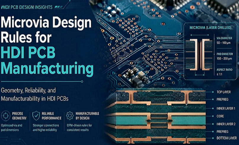
IPC uses aspect ratio and depth to define microvia geometry. A microvia should remain a blind structure with a maximum 1:1 aspect ratio and total depth not exceeding 0.25 mm. This definition matters because a deep laser via with a small opening becomes difficult to plate evenly and becomes more vulnerable to fatigue cracking.
For design review, the hdi pcb manufacturer should confirm:
- Microvia start layer and target layer
- Laser drill diameter
- Finished via diameter
- Dielectric thickness
- Copper plating thickness
- Capture pad size
- Target pad size
- Via fill requirement
- Thermal reliability test plan
Aspect Ratio Rule
Aspect ratio is calculated as dielectric depth divided by laser via diameter. A 75 micron deep dielectric with a 100 micron microvia has a 0.75:1 aspect ratio. That is easier to plate than a 90 micron deep dielectric with a 75 micron via, which reaches 1.2:1 and should be avoided for standard microvia reliability.
| Dielectric Depth | Via Diameter | Aspect Ratio | Factory View |
|---|---|---|---|
| 50 microns | 100 microns | 0.50:1 | Strong margin |
| 60 microns | 90 microns | 0.67:1 | Stable HDI range |
| 75 microns | 100 microns | 0.75:1 | Common production target |
| 80 microns | 80 microns | 1.00:1 | Upper design limit |
| 90 microns | 75 microns | 1.20:1 | High reliability risk |
A 0.75:1 aspect ratio is often a safer production target than designing at the 1:1 limit. It gives the plating process more margin and reduces thermal fatigue risk.
Via Diameter and Pad Rules
Via Diameter
Microvia diameter should be selected together with dielectric thickness. The diameter cannot be chosen only from routing density because plating quality depends on depth, wall geometry, laser cleanliness, and copper deposition.
Practical ranges:
| Microvia Class | Via Diameter | Typical Use |
|---|---|---|
| Conservative HDI | 100-125 microns | Stable production, 0.65 mm BGA |
| Standard HDI | 75-100 microns | 0.5 mm BGA, compact modules |
| Advanced HDI | 50-75 microns | 0.4 mm BGA and dense routing |
| Ultra HDI | Below 50 microns | Special process qualification |
Most hdi pcb prototype projects should avoid the smallest via unless the package density truly needs it. Smaller vias increase sensitivity to laser control, desmear, plating, and inspection.
Landing and Capture Pads
The capture pad is the pad on the layer where the microvia starts. The target pad is the pad where the microvia lands. The capture pad must be large enough to handle registration tolerance, laser position, and plating variation.
| Microvia Diameter | Typical Capture Pad | Typical Target Pad | Engineering Use |
|---|---|---|---|
| 125 microns | 300-350 microns | 250-300 microns | Conservative HDI |
| 100 microns | 250-300 microns | 225-275 microns | Standard BGA escape |
| 75 microns | 200-250 microns | 180-230 microns | Dense HDI routing |
| 50 microns | 150-200 microns | 150-180 microns | Advanced HDI review |
The capture pad should not be reduced only to win routing space. A smaller pad may route successfully in CAD but fail in registration, annular ring, or microsection inspection.
Capture Pad to Target Pad
Capture pad and target pad alignment decides whether the microvia lands safely. If the target pad is too small or misaligned, the via may create weak plating, reduced annular ring, or latent opens.
Factory review should confirm:
- Laser drill registration tolerance
- Buildup layer movement after lamination
- Capture pad diameter
- Target pad diameter
- Minimum annular ring
- Pad-to-plane clearance
- Solder mask interaction near surface pads
Annular Ring and Reliability
Annular Ring
Annular ring is the copper land remaining around a drilled or laser-drilled via. For microvias, annular ring protects registration margin and improves plating reliability.
| Design Item | Conservative Target | High-Density Target |
|---|---|---|
| Annular ring | 75 microns | 50 microns by review |
| Capture pad oversize | Via diameter + 100-150 microns | Via diameter + 75-100 microns |
| Target pad oversize | Via diameter + 80-120 microns | Via diameter + 60-90 microns |
| Plane clearance | 200-300 microns | 150-250 microns by review |
The correct annular ring depends on layer count, buildup dielectric, copper thickness, panel size, and laser registration. A high-density region may use tighter values, but the factory should confirm them before routing.
Reliability Controls
Microvia reliability is controlled by geometry, plating, thermal stress, and structure choice.
Key controls:
- Keep aspect ratio at or below 1:1.
- Prefer 0.75:1 where production margin matters.
- Avoid unnecessary stacked microvias.
- Use staggered microvias when routing space allows.
- Define copper fill when stacking is required.
- Add microsection coupons close to critical via fields.
- Run thermal stress or thermal cycling for high-reliability products.
- Use X-ray for filled or stacked structures.
Stacking vs Staggering
Staggered Vias
Staggered microvias are offset from layer to layer. They reduce direct vertical stress because each via lands on a pad that is offset from the next via.
Staggered vias are useful when:
- Routing space is available
- Production yield matters more than maximum density
- The design uses 1+N+1 or 2+N+2 structures
- BGA escape can tolerate lateral movement
- Cost control is important
| Item | Staggered Microvias |
|---|---|
| Routing density | Medium to high |
| Copper filling demand | Lower than stacked vias |
| Reliability margin | Stronger in many production builds |
| Cost | Lower than stacked structures |
| Best use | Production-friendly HDI routing |
Stacked Vias
Stacked microvias sit directly above each other. They provide higher vertical density but require stronger copper filling, planarization, and inspection.
Stacked vias are useful when:
- Inner BGA rows cannot escape otherwise
- Board outline cannot increase
- Layer transitions must stay short
- Any-layer HDI or ELIC-style routing is required
- Dense processor, memory, or AI modules drive the layout
| Item | Stacked Microvias |
|---|---|
| Routing density | Very high |
| Copper filling demand | Required |
| Reliability margin | Process-dependent |
| Cost | Higher |
| Inspection | Microsection and X-ray strongly required |
Staggered vs Stacked
| Decision Factor | Staggered Vias | Stacked Vias |
|---|---|---|
| Density | High | Highest |
| Cost | Lower | Higher |
| Process risk | Lower | Higher |
| Copper fill | Often limited | Required for reliable stacking |
| Best fit | 0.5 mm BGA with space | 0.4 mm BGA or tighter |
| Factory control | Registration and plating | Fill, cap, plating, microsection |
The safest engineering rule is simple: use staggered vias when they fit, and use stacked vias only when the density requires them.
Via-in-Pad Rules
Via-in-Pad
Via-in-pad places a microvia inside the component pad. VIPPO, or via-in-pad plated over, fills and caps the via so the pad remains solderable.
Via-in-pad is used for:
- 0.5 mm and 0.4 mm BGA fanout
- Dense power pin breakout
- Short decoupling paths
- High-speed transition control
- Compact module design
| VIP Design Item | Practical Target | Risk Controlled |
|---|---|---|
| Microvia diameter | 75-125 microns | Fill and plating reliability |
| Dimple after planarization | Below 10-15 microns | Uneven solder volume |
| Copper cap | Continuous plated cap | Solder wicking |
| Finish | ENIG or equivalent flat finish | Fine-pitch assembly |
| Inspection | X-ray and microsection | Hidden fill defects |
Via-in-pad should not be used everywhere by default. It adds filling, planarization, plating, inspection, and cost.
Via-in-Pad Failure Modes
Common failure modes include:
- Solder wicking into an unfilled via
- Dimple causing uneven solder joint height
- BGA void concentration above the via
- Copper cap cracking after reflow
- Incomplete filling under X-ray
- Poor planarity under fine-pitch packages
These failures often appear at the PCBA stage, not during bare-board electrical test.
Laser Processing
Laser Drilling
Laser processing creates microvias through thin dielectric. A stable laser process must control energy, spot size, pulse count, debris removal, and copper stop condition.
Laser process checks:
- Via entrance diameter
- Via bottom diameter
- Taper shape
- Glass fiber exposure
- Resin residue
- Target pad damage
- Plating continuity
- Copper adhesion
A microvia is only as reliable as the surface preparation after drilling. If residue remains at the bottom, plating can look acceptable at first but separate after thermal stress.
Plating and Filling
Microvia plating must deposit copper evenly from the capture pad to the target pad. For stacked vias or via-in-pad, copper filling becomes more important.
Factory controls:
- Desmear and via cleaning
- Electroless copper activation
- Copper plating thickness
- Void inspection
- Filled via planarity
- Microsection frequency
- Thermal stress validation
Stack-Up Co-design
Microvia and Stack-Up
Microvia PCB design rules must be co-designed with the stack-up. The dielectric thickness, material type, copper weight, and lamination sequence decide whether the via geometry is realistic.
Stack-up data should include:
- Layer count
- HDI type: 1+N+1, 2+N+2, 3+N+3, or any-layer
- Microvia layer pairs
- Buried via layer pairs
- Through via rules
- Buildup dielectric thickness
- Copper thickness
- Controlled impedance layers
- Material family
- Surface finish
- Final thickness
Material and Impedance
High speed hdi circuit boards need material and impedance control before layout.
Common targets:
| Signal Type | Typical Impedance | Stack-Up Control |
|---|---|---|
| Single-ended clock | 50 ohm | Trace width and reference plane |
| USB differential | 90 ohm | Pair spacing and dielectric thickness |
| Ethernet / LVDS | 100 ohm | Differential geometry and return path |
| PCIe differential | 85 ohm | Material loss and via transition |
| RF control | 50 ohm | Low-loss material and copper roughness |
Controlled impedance cannot be fixed after the board is routed. It must be built into stack-up, material, copper, solder mask, and coupon design.
Benchuang Electronics Capability
Microvia PCB Capability
Benchuang Electronics should be evaluated as an hdi pcb manufacturer for microvia PCB, high density interconnect boards, fine-pitch fanout, hdi pcb prototype builds, and production transfer. Public company information describes Benchuang Electronics as a manufacturer focused on advanced interconnect solutions, including rigid, flex, rigid-flex, high-frequency, high-reliability, HDI, and ultra HDI printed circuit boards.
Engineering review should focus on:
- Microvia diameter capability
- 1+N+1 and 2+N+2 stack-up support
- Via-in-pad filling and cap plating
- Controlled impedance tolerance
- TDR test method
- IPC Class 2 and Class 3 support
- X-ray and microsection inspection
- Prototype-to-production yield tracking
Capability Fit Questions
Before sending a microvia PCB project, engineers should ask:
- Is the target microvia diameter inside the stable process range?
- Is the dielectric depth compatible with a 1:1 or lower aspect ratio?
- Can staggered vias replace stacked vias?
- Does via-in-pad require copper filling or nonconductive filling?
- What dimple limit is used after planarization?
- How many sequential lamination cycles are required?
- Which coupons will be added to verify microvia plating?
- Can the same stack-up move from hdi pcb prototype to production?
Manufacturing Best Practices
DFM Release Package
A microvia PCB release package should include more than Gerber files.
Required data:
- Gerber, ODB++, or IPC-2581 files
- Excellon mechanical drill file
- Laser drill file
- Stack-up drawing
- Via structure map
- Microvia diameter and pad sizes
- Via-in-pad fill and cap requirements
- Controlled impedance table
- Material callout
- Copper thickness by layer
- IPC class
- Inspection coupon requirements
- Surface finish
- Assembly notes for BGA or fine-pitch parts
Quality Control Plan
A strong quality plan should include:
- CAM and DFM review
- Inner-layer AOI
- Lamination registration measurement
- Laser drilling inspection
- Desmear quality check
- Copper plating thickness check
- Microsection for critical microvia fields
- X-ray for filled or stacked microvias
- 100% electrical test
- Impedance coupon TDR test
- Solder mask registration inspection
- Warpage check after thermal simulation
Two Key Comparisons
Blind Via vs Microvia
| Item | Blind Via | Microvia |
|---|---|---|
| Drilling method | Mechanical or laser | Usually laser |
| Diameter | Larger | Smaller |
| Depth | Can be deeper | Maximum 0.25 mm by IPC definition |
| Aspect ratio | Higher possible | Maximum 1:1 |
| Best use | General blind connection | HDI fanout and fine-pitch routing |
| Main risk | Registration and plating | Plating fatigue and thermal stress |
Via-in-Pad vs Dogbone Fanout
| Item | Via-in-Pad | Dogbone Fanout |
|---|---|---|
| Best pitch | 0.5 mm and below | 0.8 mm and larger |
| Routing density | High | Moderate |
| Cost | Higher | Lower |
| Assembly risk | Requires fill and cap | Lower if spacing allows |
| Signal path | Shorter | Longer |
| Best use | Dense BGA and compact modules | Standard BGA routing |
Real Factory Case
Project Background
A wearable health sensor used a 0.5 mm BGA microcontroller, BLE radio, battery charging IC, 6-axis sensor, flash memory, and two board-to-board connectors. The first PCB concept used a standard 6-layer board with 0.20 mm mechanical vias.
| Item | Original Concept | Microvia PCB Revision |
|---|---|---|
| Board type | Standard multilayer PCB | HDI microvia PCB |
| Layer count | 6 layers | 8 layers |
| HDI structure | None | 1+6+1 |
| Board thickness | 0.80 mm | 0.80 mm |
| Trace / space | 100/100 microns | 75/75 microns, 50/50 microns local |
| Via type | 0.20 mm through vias | 90 micron microvias |
| BGA pitch | 0.5 mm | 0.5 mm |
| Finish | ENIG | ENIG |
| Impedance | Not fully controlled | 50 ohm RF, 90 ohm USB |
| Inspection | AOI and E-test | AOI, E-test, X-ray, microsection, impedance coupon |
Problem Found
The standard concept routed the outer BGA rows, but the inner rows forced long detours. The RF line crossed a split reference area, and the charger thermal pad lacked enough copper spreading. During the first hdi pcb prototype build, the board passed E-test, but 6 of 80 assembled units failed BLE range testing after a 60 C thermal soak.
Root causes:
- One RF transition used a microvia with insufficient nearby ground stitching.
- A local 50/50 micron region was placed on thicker copper than the factory preferred.
- Two microvias were designed at an aspect ratio close to 1.1:1 because dielectric thickness changed late.
- The impedance coupon did not match the final solder mask condition.
- The charger copper area was unbalanced near one board edge.
Corrective Actions
The revised pilot changed:
- Microvia dielectric depth reduced from 85 microns to 70 microns.
- Microvia diameter increased from 75 microns to 90 microns.
- Aspect ratio moved from about 1.1:1 to 0.78:1.
- Ground stitching was added near RF layer transitions.
- Local fine-line copper was changed to 12 microns.
- Impedance coupon was rebuilt to include final solder mask.
- Copper thieving was added near the charger zone.
| Metric | First HDI Prototype | Revised Pilot |
|---|---|---|
| BLE thermal-soak failures | 6/80 | 0/160 |
| Microvia suspect sites | 4 sites | 0 sites |
| RF impedance deviation | +9% | +2.6% |
| Local warpage | 0.36 mm | 0.18 mm |
| First-pass functional yield | 90.0% | 98.1% |
This result came from microvia geometry correction, not from simply adding more layers. The key was matching via diameter, dielectric depth, material, impedance coupon, and local copper balance.
Common Design Errors
Microvia Geometry Errors
- Designing above 1:1 aspect ratio
- Shrinking capture pads without factory approval
- Ignoring target pad size
- Using the same microvia size for every layer pair
- Changing dielectric thickness after layout
- Missing annular ring requirements
Stack-Up Errors
- Routing before stack-up approval
- Using stacked vias where staggered vias fit
- Forgetting the laser drill file
- Missing via structure map
- Mixing blind, buried, and microvias without lamination sequence
- Choosing any-layer HDI without density need
Manufacturing Errors
- No microsection coupon near critical via fields
- No X-ray plan for stacked or filled vias
- Missing via-in-pad fill and cap notes
- No dimple limit for VIPPO
- Using 35 micron copper in dense 50/50 micron areas
- Treating PCB E-test as proof of PCBA reliability
PCB is the bare printed circuit board. PCA is the assembled board with components, solder joints, firmware, labels, inspection data, and functional test records. A microvia PCB can pass bare-board E-test but fail at PCA level if soldering, thermal stress, or high-speed margins are not controlled.
FAQ About Microvia PCB Design Rules
Question: What is a Microvia PCB?
Answer: A Microvia PCB is an HDI printed circuit board that uses laser-drilled blind vias to connect adjacent or shallow layers. Microvias help route fine-pitch BGA packages, reduce via stubs, improve density, and create shorter signal transitions than standard through vias.
Question: What is the correct microvia aspect ratio?
Answer: The IPC-related definition sets a maximum microvia aspect ratio of 1:1 and a total depth of no more than 0.25 mm. In production, many engineers target around 0.75:1 for better plating margin and thermal reliability.
Question: Should microvias be stacked or staggered?
Answer: Staggered microvias should be used when routing space allows because they usually provide better production margin and lower cost. Stacked microvias should be used when the layout needs maximum vertical density, but they require copper filling, microsection inspection, and tighter process control.
Question: When is via-in-pad required?
Answer: Via-in-pad is often required for 0.5 mm and 0.4 mm BGA packages, dense power pin breakout, short decoupling paths, and compact hdi circuit boards. It must include fill, cap plating, dimple control, and X-ray or microsection inspection when reliability matters.


![Understanding PCB Costs & Pricing [Your Complete Guide]](https://hdicircuitboard.com/wp-content/uploads/elementor/thumbs/Understanding-PCB-Costs-Pricing-Your-Complete-Guide-qzzhe6mcaxuolkux3xalfktgavumi9y1aqfbs9bpv4.webp "Understanding PCB Costs & Pricing [Your Complete Guide]")


