
Signal integrity in high speed pcb design determines the reliability of data transmission, as high-frequency signals (≥1Gbps) are prone to reflections, crosstalk, and attenuation. This guide addresses core challenges, provides actionable fixes with precise production parameters, and aligns with IPC standards to ensure compatibility with hdi pcb, Low Loss PCB, and ultra low loss pcb applications.
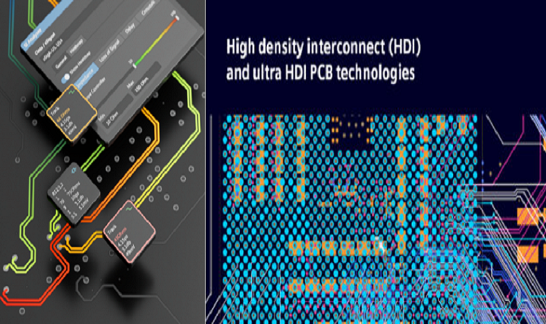
Learn more about: Signal Integrity in HDI PCB Design
Signal Integrity in High Speed PCB: Core Concepts
Definition & Critical Thresholds
- Signal integrity (SI) refers to a signal’s ability to retain fidelity from transmitter to receiver, measured by eye diagram height (≥0.3Vpp) and jitter (≤10% of bit period).
- High-speed signals are classified by edge rate (≥1V/ns) or data rate (≥1Gbps), requiring transmission line treatment when trace length exceeds λ/10 (λ = signal wavelength).
- Compliance with IPC-2221 and IPC-6012 Class 3 is mandatory for high-reliability applications (aerospace, medical devices).
Impact of Material Selection
- Low Loss PCB (Df=0.004–0.009 @10GHz) supports 5–25Gbps, while ultra low loss pcb (Df≤0.004) enables ≥25Gbps with 40% lower insertion loss.
- Dielectric constant (εr) stability: FR-4 (εr=4.0–4.7) degrades above 5GHz, while Rogers RO4350B (εr=3.5) remains stable up to 15GHz.
- hdi pcb requires materials with low CTE (X/Y ≤16ppm/°C) to prevent warpage during sequential lamination.
Learn more about: High-Speed PCB Materials: A Complete Comparison Guide
High Speed Signal Integrity Challenges
Signal Reflection
- Cause: Impedance mismatches (±5% tolerance violation) from trace width changes, vias, or unterminated lines.
- Impact: Ringing (±15% signal amplitude) and overshoot/undershoot, leading to bit errors at ≥10Gbps.
- Quantification: TDR measurements show reflection coefficient >0.1 indicates critical mismatch (IPC-TM-650 2.5.5.12).
Crosstalk/Coupling
- Types: Horizontal (same-layer, 3W rule violation) and vertical (inter-layer, broadside coupling).
- Critical Threshold: Crosstalk >-25dB disrupts signal integrity for high speed pcb (≥10Gbps).
- Contributing Factors: Trace spacing <3x width, parallel runs >500mil, and missing ground planes between signal layers.
Ground Bounce/Switching Noise
- Mechanism: Simultaneous switching of ≥8 I/O pins creates voltage spikes (≥100mV) due to parasitic inductance in ground paths.
- HDI PCB Risk: Microvia clusters increase loop inductance by 60%, exacerbating bounce in dense layouts.
- Measurement: IPC-6016 requires ground bounce ≤5% of supply voltage for Class 3 designs.
Attenuation & Loss
- Dielectric Loss: Dominates above 10GHz—ultra low loss pcb (e.g., Megtron 7) reduces loss by 30% vs. standard FR-4.
- Skin Effect: At 50GHz, current concentrates in 1.2μm copper surface, requiring thick copper (≥2oz) for trace conductivity.
- Insertion Loss Target: ≤0.3dB/inch @20GHz for ultra low loss pcb (IPC-4103A).
Essential SI Design Guidelines
Controlled Impedance
- Target Values: 50Ω (single-ended, ±5% tolerance) and 90–100Ω (differential pairs, ±5% tolerance) per IPC-2221.
- Calculation Parameters: Trace width (4mil for 50Ω microstrip on 0.4mm FR-4), dielectric thickness (0.2mm), and copper weight (1oz).
- Manufacturing Control: Impedance coupons (100mm length) included on every panel for TDR validation.
Learn more about: 50Ω / 75Ω / 100Ω Impedance in High Density Interconnect (HDI) PCBs: Design & Production Guide
Solid Return Paths
- Ground Plane Design: Continuous planes with ≤50mil gaps; stitching vias (1mm pitch) to connect split planes.
- HDI PCB Requirement: Adjacent ground planes for signal layers in 1+N+1 stackup to reduce loop inductance.
- Return Via Placement: Within 20mil of signal vias to minimize inductance (≤1.2nH per via).
Trace Length Matching
- Differential Pairs: Length mismatch ≤5mil (≤25ps skew) for ≥10Gbps signals.
- Clock Signals: Skew ≤10ps between clock and data lines to meet setup/hold requirements.
- Tuning Method: Serpentine traces with pitch ≥5x width to avoid impedance discontinuities.
Component Placement
- Decoupling Capacitors: 0402/0201 packages placed ≤0.5cm from IC power pins (ESL ≤1nH).
- Sensitive Components: Analog/digital separation by ≥3mm; clock oscillators placed ≥10mm from high-speed data lines.
- hdi pcb Specific: BGA components (≤0.8mm pitch) use microvia fanout (0.15mm vias) to minimize stub length.
Layer Stackup Design
- High Speed PCB: Microstrip (outer layers) for 50Ω single-ended; stripline (inner layers) for differential pairs (100Ω).
- HDI PCB: 2+N+2 stackup with alternating signal/ground planes; dielectric thickness ≤0.1mm between signal and ground.
- Symmetry Requirement: Balanced layer counts (e.g., 12-layer: 4 signal + 2 power + 2 ground) to prevent warpage (≤0.3mm/m).
Key Comparisons
| Solution | Application | Performance Gain | Cost Impact |
|---|---|---|---|
| FR-4 Material | ≤5Gbps High Speed PCB | Baseline | Low (+0%) |
| Low Loss PCB (FR408HR) | 5–25Gbps | -20% insertion loss | Medium (+25%) |
| Ultra Low Loss PCB (Rogers RO4350B) | ≥25Gbps | -40% insertion loss | High (+70%) |
| Microstrip Routing | Outer Layers | Simplified manufacturing | Low (+0%) |
| Stripline Routing | Inner Layers | -35dB crosstalk reduction | Medium (+15%) |
| Challenge | FR-4 Solution | Ultra Low Loss PCB Solution |
|---|---|---|
| Signal Reflection | Series termination (50Ω) | Impedance-controlled traces + back-drilled vias |
| Crosstalk | 3W rule + guard traces | 5W rule + ground planes between layers |
| Attenuation | Short trace lengths (<3in) | Low Df material + thick copper (2oz) |
Quality Control & Validation
Testing Protocols
- TDR Impedance Testing: Verify trace impedance within ±3% of target (IPC-TM-650 2.5.5.12).
- Eye Diagram Analysis: Eye height ≥0.3Vpp and jitter ≤35ps for 50Gbps signals (CISPR 22 Class B).
- Thermal Cycling: 1000 cycles (-40°C~125°C) with no layer separation (IPC-TM-650 2.6.7.2).
Manufacturing Checks
- Trace Width/Spacing: ±0.5mil tolerance (IPC-2221) to maintain impedance.
- Via Quality: Microvia diameter 0.1–0.15mm, aspect ratio ≤1:1 (IPC-6016).
- Material Verification: Df/Dk testing of laminate batches (IPC-TM-650 2.5.5.12) for ultra low loss pcb.
Factory Case Study: 16-Layer HDI Ultra Low Loss PCB
Project Specifications
- Layers: 16 (4+8+4 stackup), data rate: 50Gbps (NRZ), material: Rogers RO4350B (Df=0.0037 @10GHz).
- Impedance targets: 50Ω (single-ended), 100Ω (differential), hdi pcb with stacked microvias (0.12mm diameter).
Issues Encountered
- Crosstalk (+18dB) between adjacent differential pairs (spacing=2x width).
- Ground bounce (120mV) from 16 simultaneous switching I/O pins.
- Insertion loss (0.4dB/inch @20GHz) exceeding target (0.3dB/inch).
Improvements Implemented
- Increased pair spacing to 3x width, adding guard traces (50Ω) between sensitive nets.
- Added 0.1μF decoupling capacitors (0402) every 1.5cm, with return vias within 15mil of signal vias.
- Switched to 2oz copper traces and optimized stripline stackup (dielectric thickness=0.08mm).
Results
- Crosstalk reduced to -32dB, meeting IPC requirements.
- Ground bounce ≤75mV, within 5% of 1.5V supply.
- Insertion loss improved to 0.28dB/inch @20GHz.
- Manufacturing yield: 97.8% (up from 83% initial run).
| Case Study Aspect | Details / Parameters |
|---|---|
| Project Specifications |
• Layers: 16 (4+8+4 stackup) • Data rate: 50Gbps (NRZ) • Material: Rogers RO4350B (Df=0.0037 @10GHz) • Impedance targets: 50Ω (single-ended), 100Ω (differential) • HDI PCB: Stacked microvias (0.12mm diameter) |
| Issues Encountered |
• Crosstalk (+18dB): Adjacent differential pairs (spacing=2x width) • Ground bounce (120mV): 16 simultaneous switching I/O pins • Insertion loss: 0.4dB/inch @20GHz (target=0.3dB/inch) |
| Improvements Implemented |
• Increased pair spacing to 3x width + 50Ω guard traces • 0.1μF decoupling capacitors (0402) every 1.5cm + return vias (15mil from signal vias) • 2oz copper traces + stripline stackup (dielectric thickness=0.08mm) |
| Results |
• Crosstalk reduced to -32dB (IPC compliant) • Ground bounce ≤75mV (≤5% of 1.5V supply) • Insertion loss: 0.28dB/inch @20GHz • Manufacturing yield: 97.8% (up from 83%) |
Common Design Errors
- Inadequate Ground Planes: Split ground planes under differential pairs increase crosstalk by 15x—requires copper filling (cost +$0.60/board).
- Unterminated Traces: Unterminated high-speed lines (≥10Gbps) cause reflections—factory rework adds 3–5 days to lead time.
- Via Stub Neglect: Via stubs >10mil for 25Gbps signals increase reflection loss by 20%—back-drilling required (cost +$0.30/via).
- Material Mismatch: Using FR-4 for ≥25Gbps designs leads to 30% higher attenuation—requires full board redesign.
FAQ
Q1: What’s the difference between Low Loss PCB and ultra low loss pcb for high speed applications?
A1: Low Loss PCB (Df=0.004–0.009 @10GHz) works for 5–25Gbps with cost-effective performance, while ultra low loss pcb (Df≤0.004) supports ≥25Gbps (e.g., 50Gbps data center switches) and maintains stable impedance up to 40GHz, ideal for hdi pcb and high-frequency RF designs.
Q2: How to reduce ground bounce in dense hdi pcb layouts?
A2: Use multiple ground pins per IC (1 ground pin for every 2 signal pins), place decoupling capacitors ≤0.5cm from power pins, and implement interleaved power/ground vias (1mm pitch) to reduce loop inductance. For 16-layer hdi pcb, split power planes into smaller segments to isolate switching noise.
Q3: What trace spacing is required for high speed pcb (25Gbps) to avoid crosstalk?
A3: Maintain trace spacing ≥5x width (e.g., 20mil spacing for 4mil width) for 25Gbps signals. For hdi pcb with limited space, use guard traces (50Ω) grounded every 500mil to reduce crosstalk by 25dB, ensuring compliance with IPC-2221.
Q4: When should I use stripline vs. microstrip routing for high speed pcb?
A4: Stripline (inner layers, sandwiched between ground planes) is preferred for ≥25Gbps signals, reducing crosstalk by 35dB vs. microstrip. Microstrip (outer layers) is suitable for ≤10Gbps designs, offering easier access for testing and lower manufacturing cost—ideal for non-critical high speed pcb paths.
If you need high speed PCB manufacturing or design support,our engineering team provides free DFM analysis and quotation.


![Understanding PCB Costs & Pricing [Your Complete Guide]](https://hdicircuitboard.com/wp-content/uploads/elementor/thumbs/Understanding-PCB-Costs-Pricing-Your-Complete-Guide-qzzhe6mcaxuolkux3xalfktgavumi9y1aqfbs9bpv4.webp "Understanding PCB Costs & Pricing [Your Complete Guide]")


