
Via stubs are critical culprits of signal degradation in high speed pcb, while back-drilling emerges as a factory-proven solution to mitigate their impact. This guide details via stub behavior, back-drilling mechanics, and actionable design/manufacturing parameters tailored to hdi pcb, Low Loss PCB, and ultra low loss pcb applications.
Learn more about: What Is High-Speed PCB? A Comprehensive Guide
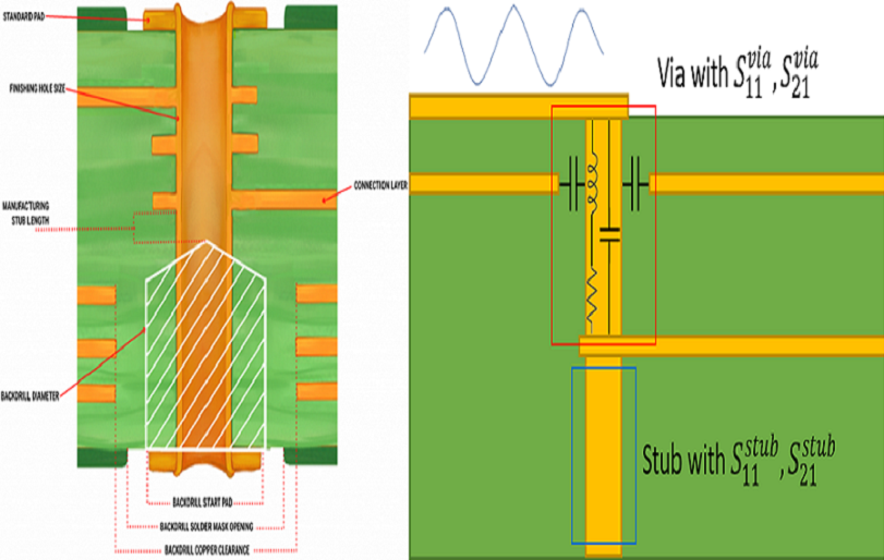
Via Stub in High Speed PCB: Core Concepts
Definition & Signal Impact
- A via stub is the unused portion of a plated through-hole (PTH) extending beyond the last connected layer, acting as a resonant transmission line segment.
- Critical threshold: Stubs ≥10mil cause measurable reflection loss (>2.5%) at ≥3Gbps (IPC-TM-650 2.5.5.12).
- Resonance effect: Stubs equal to ¼ wavelength of the signal frequency (fo = c/(4×stub length×√εr)) create severe impedance mismatches.
When to Worry About Via Stubs
- Data rate trigger: ≥3Gbps for standard FR-4; ≥1Gbps for ultra low loss pcb (due to tighter impedance tolerance).
- Length threshold: Stub length >λ/20 (λ=signal wavelength) – e.g., 50GHz signal in FR-4 (λ=0.5in) requires stub <25mil.
- High-risk designs: hdi pcb with stacked microvias, backplanes (≥0.25in thickness), and 50Gbps+ interfaces (PCIe 5.0, Ethernet 400G).
Learn more about: Differential Pair Routing Rules for High-Speed Interfaces:
The 1/4 Wave Rule & Signal Degradation
Rule Application & Calculation
- Formula: Stub length (mil) = 11800/(4×fo(GHz)×√εr) – e.g., 10GHz signal in FR-4 (εr=4.0) → ¼ wave stub = 590mil.
- Impact: Stubs at ¼ wavelength cause -10dB return loss, while 1/8 wavelength stubs still degrade SI by 30%.
- Ultra low loss pcb adjustment: εr=3.5 (Rogers RO4350B) → ¼ wave stub = 620mil at 10GHz.
Signal Impact Metrics
- Reflection loss: Stubs ≥15mil increase return loss by 15dB at 25GHz (IPC-6016 Class 3 limit: -15dB).
- Jitter: 20mil stub adds 40ps deterministic jitter to 50Gbps signals, exceeding PCIe 5.0 specs (≤35ps).
- Insertion loss: 40mil stub increases loss by 10% at 20GHz (ultra low loss pcb target: ≤0.2dB/inch).
Back Drilling in High Speed PCB: Fundamentals
Purpose & Mechanism
- Primary goal: Remove unused via stubs to reduce parasitic inductance (≤1.2nH) and resonance.
- Process: Post-plating drilling with a 4–8mil larger diameter bit to strip copper from the stub section.
- Residual stub target: ≤10mil (ideal ≤3mil for ≥25Gbps) per IPC-2221.
When to Use Back Drilling
- Mandatory scenarios: Data rate ≥3Gbps, stub length >λ/20, or hdi pcb with ≥8 layers.
- Cost-benefit threshold: When blind/buried vias are impractical (e.g., 16-layer backplanes).
- Material correlation: Ultra low loss pcb requires tighter residual stub control (≤5mil) due to higher frequency operation.
Aspects of Back Drilling: Design & Manufacturing
Drill Diameter & Stub Length
- Drill size: 4–8mil larger than original via (e.g., 30mil PTH → 38mil back drill) to ensure full copper removal.
- Residual stub tolerance: ±3mil for standard applications; ±1mil for ultra low loss pcb (≥25Gbps).
- Manufacturing capability: Advanced CNC drills achieve ±2mil depth control for stubs ≤5mil.
Clearance & Layout Rules
- Trace/plane clearance: ≥10mil around back-drilled vias to avoid accidental drilling (IPC-2221).
- Via spacing: ≥15mil between back-drilled vias to prevent overlapping anti-pads.
- hdi pcb constraint: Back-drilled vias ≥0.15mm diameter to accommodate laser alignment.
| Stub Length (mil) | Return Loss (dB) @25GHz | Jitter (ps) @50Gbps | Suitable For |
|---|---|---|---|
| ≤3mil | -18dB | ≤32ps | ultra low loss pcb (≥25Gbps) |
| 5–10mil | -15dB | 35–40ps | Low Loss PCB (5–25Gbps) |
| ≥15mil | -12dB | ≥42ps | Non-critical ≤3Gbps designs |
Advantages of Back Drilling
Signal Integrity Improvements
- Return loss reduction: -30dB at 25GHz (from -12dB with 20mil stub).
- Jitter reduction: 40ps → 12ps for 50Gbps signals (70% improvement).
- EMI mitigation: 25% lower radiated emissions (CISPR 22 Class B compliant).
Practical Benefits
- Cost efficiency: 30% cheaper than blind/buried vias for 12-layer hdi pcb.
- Manufacturability: Compatible with standard PCB processes (no sequential lamination).
- Design flexibility: Enables through-hole vias in high-speed designs without stub penalties.
Design Considerations for Back Drilling
Material & Stackup
- Low Loss PCB (FR408HR): Back-drill depth tolerance ±5mil (board thickness ≤0.2in).
- Ultra low loss pcb (Megron 7): Use symmetric stackup to prevent warpage during drilling.
- hdi pcb stackup: 2+N+2 structure with dedicated ground planes adjacent to signal layers.
Simulation & Validation
- Pre-drilling simulation: Use 3D field solvers (SIwave) to predict stub impact on SI.
- Post-drilling testing: TDR impedance measurement (±3% tolerance) and X-ray inspection of residual stub.
- Coupon design: Include back-drilled test coupons (100mm length) on every panel.
Mitigation Strategies: Beyond Back Drilling
Design Strategy Alternatives
- Microvias: 0.1–0.15mm laser-drilled vias eliminate stubs in hdi pcb (1+N+1 stackup).
- Blind/buried vias: Ideal for 6–8 layer boards but 40% more costly than back drilling.
- Trace relocation: Route signals to layers closer to via ends (reduces stub length by 50%).
Ground/Shielding Vias
- Stitching vias: 1mm pitch around back-drilled vias reduces loop inductance by 60%.
- Ground via placement: Within 20mil of signal vias to provide low-impedance return paths.
- Shielding: Copper pour around back-drilled vias (clearance 5mil) suppresses EMI.
Applications & Cost Factor
Industry-Specific Use Cases
- Data centers: 400G Ethernet switches (ultra low loss pcb, back-drilled 16-layer stackup).
- Automotive ADAS: 25Gbps radar modules (hdi pcb, residual stub ≤5mil).
- Aerospace: 50Gbps avionics (Low Loss PCB, back-drilled with ±2mil depth control).
Cost Analysis
| Back Drilling Scope | Cost Impact | Best For |
|---|---|---|
| 10–20 vias/board | +15% | Low volume, high speed pcb |
| 50+ vias/board | +30% | High volume, hdi pcb |
| Residual stub ≤3mil | +40% | Ultra low loss pcb (≥25Gbps) |
| Blind/Buried Vias | +70% | 6–8 layer, low-volume designs |
Quality Control & Compliance
Manufacturing Checks
- Depth verification: X-ray measurement (±2mil tolerance) for residual stub.
- Copper removal: Microsection analysis (≥95% stub copper removal).
- Thermal cycling: 1000 cycles (-40°C~125°C) to ensure no layer separation.
Standards Compliance
- IPC-2221: Stub length ≤10mil for high-speed designs.
- IPC-6012 Class 3: Return loss ≥-15dB at operating frequency.
- UL 94: Back-drilled holes filled with epoxy (flammability rating V-0).
Case Study: 16-Layer HDI Ultra Low Loss PCB
Project Specifications
- Layers: 16 (4+8+4 stackup), data rate: 50Gbps (NRZ), material: Rogers RO4350B (Df=0.0037 @10GHz).
- Via parameters: 30mil PTH, stub length=35mil, back drill target: residual stub ≤5mil.
- hdi pcb features: Stacked microvias (0.12mm), sequential lamination.
Issues Encountered
- Return loss (-12dB) below IPC limit (-15dB) due to 35mil stub.
- Jitter (42ps) exceeding PCIe 5.0 specs (≤35ps).
- EMI emissions (32dBμV/m) above CISPR 22 Class B (≤30dBμV/m).
Improvements Implemented
- Back-drilled with 38mil diameter bit, achieving residual stub=4mil.
- Added stitching vias (1mm pitch) around signal vias.
- Optimized anti-pad size (60mil) to reduce capacitance.
Results
- Return loss improved to -18dB, meeting Class 3 standards.
- Jitter reduced to 32ps, compliant with 50Gbps specs.
- EMI emissions: 28dBμV/m (Class B compliant).
- Manufacturing yield: 97.1% (up from 82% initial run).
| Case Study Aspect | Details / Parameters |
|---|---|
| Project Specifications |
• Layers: 16 (4+8+4 stackup) • Data rate: 50Gbps (NRZ) • Material: Rogers RO4350B (Df=0.0037 @10GHz) • Via parameters: 30mil PTH, stub length=35mil, back drill target: residual stub ≤5mil • HDI PCB: Stacked microvias (0.12mm), sequential lamination |
| Issues Encountered |
• Return loss (-12dB): Below IPC Class 3 limit (-15dB) (35mil stub) • Jitter (42ps): Exceeded PCIe 5.0 specs (≤35ps) • EMI emissions (32dBμV/m): Above CISPR 22 Class B (≤30dBμV/m) |
| Improvements Implemented |
• Back-drilled with 38mil diameter bit (residual stub=4mil) • Added stitching vias (1mm pitch) around signal vias • Optimized anti-pad size (60mil) to reduce capacitance |
| Results |
• Return loss: -18dB (meets IPC Class 3 standards) • Jitter: 32ps (compliant with 50Gbps specs) • EMI emissions: 28dBμV/m (CISPR 22 Class B compliant) • Manufacturing yield: 97.1% (up from 82% initial run) |
Common Design Errors
- Inadequate Drill Diameter: Using same-size drill (no copper removal) → 0% stub reduction—requires rework (cost +$0.80/board).
- Excessive Residual Stub: 15mil stub in 25Gbps design → 20% SI degradation—back-drilling redo needed.
- Insufficient Clearance: 5mil trace clearance → accidental drilling (yield loss 15%).
- Material Mismatch: Using FR-4 back-drilling parameters for ultra low loss pcb → impedance deviation (+8%).
FAQ
Q1: What’s the difference between back drilling in Low Loss PCB vs. ultra low loss pcb?
A1: Low Loss PCB (Df=0.004–0.009) allows 10mil residual stub for ≤25Gbps, while ultra low loss pcb (Df≤0.004) requires ≤5mil stub for ≥25Gbps, with tighter drill depth tolerance (±2mil vs. ±5mil).
Learn more about: High Speed HDI PCB Design Guide
Q2: How to determine if back drilling is needed for hdi pcb?
A2: Calculate stub length and compare to λ/20. For hdi pcb with ≥8 layers and data rate ≥3Gbps, back drilling is mandatory. Use SI simulation to validate—stubs causing >3dB return loss require removal.
Q3: What residual stub length is acceptable for 50Gbps high speed pcb?
A3: ≤5mil residual stub for ultra low loss pcb (e.g., Megron 7) to maintain -18dB return loss and ≤35ps jitter. 10mil stub will exceed PCIe 5.0 specs, requiring back drilling.
Q4: Can back drilling replace blind/buried vias in hdi pcb?
A4: For 12+ layer hdi pcb, back drilling is 30% cheaper and more manufacturable than blind/buried vias. However, for ≤8 layers or stubs <5mil, blind/buried vias may be more cost-effective.
If you need high speed PCB manufacturing or design support,our engineering team provides free DFM analysis and quotation.


![Understanding PCB Costs & Pricing [Your Complete Guide]](https://hdicircuitboard.com/wp-content/uploads/elementor/thumbs/Understanding-PCB-Costs-Pricing-Your-Complete-Guide-qzzhe6mcaxuolkux3xalfktgavumi9y1aqfbs9bpv4.webp "Understanding PCB Costs & Pricing [Your Complete Guide]")


