
High speed pcb layer stackup design is the foundation of signal integrity, power delivery, and EMI control, requiring precise symmetry, layer arrangement, and material selection. This guide details factory-proven guidelines, actionable parameters, and real-world examples tailored to hdi pcb, Low Loss PCB, and ultra low loss pcb applications.
Learn more about : What Is High-Speed PCB? A Comprehensive Guide
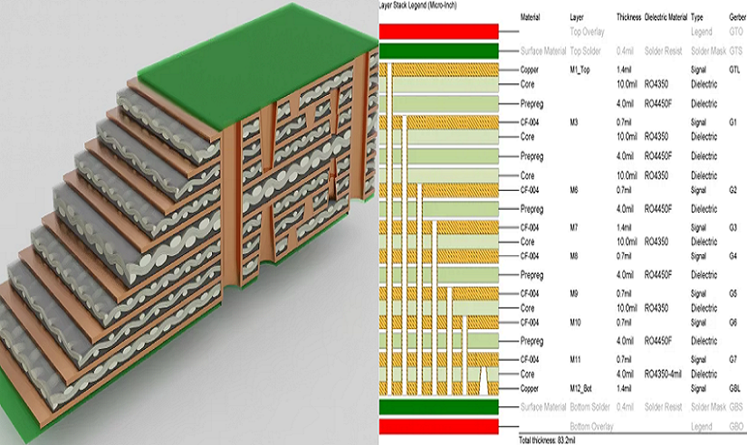
High Speed PCB Stackup Design: Core Concepts
Definition & Critical Role
- A layer stackup refers to the ordered arrangement of signal, power, and ground layers separated by dielectric materials, defining the PCB’s electrical and mechanical properties.
- Critical threshold: For signals ≥1Gbps, stackup directly impacts impedance control (±5% tolerance per IPC-2221) and crosstalk (-35dB target).
- High-speed mandate: Stackup must be finalized before routing to ensure controlled impedance, solid return paths, and minimal EMI (IPC-6012 Class 3).
Impact on Performance Metrics
- Signal integrity: Proper stackup reduces insertion loss by 30% (ultra low loss pcb target: ≤0.2dB/inch @20GHz).
- Power integrity: Adjacent power/ground planes provide 32.7pF/in² capacitance (FR-4, 0.2mm spacing) for noise suppression.
- Mechanical stability: Symmetric stackup limits warpage to ≤0.3mm/m (critical for hdi pcb sequential lamination).
Learn more about: High-Speed PCB Materials: A Complete Comparison Guide
Guidelines for High Speed Stackups
Symmetry & Layer Arrangement
- Symmetry rule: Mirror inner layers around the center (e.g., 12-layer: Signal-GND-Power-Signal-Signal-Power-GND-Signal) to prevent warpage.
- Layer count: Minimum 4 layers for high speed pcb; 8+ layers for hdi pcb (1+N+1 stackup) to support dense routing.
- Lamination cycles: ≤3 sequential lamination cycles for hdi pcb to avoid layer separation (IPC-6016).
Avoid Adjacent Signals & Solid Ground Planes
- Signal layer separation: No adjacent signal layers—separate with ground/power planes to reduce crosstalk by 40%.
- Ground plane requirements: Solid planes with ≤50mil gaps; stitching vias (1mm pitch) to connect split planes.
- hdi pcb specific: Dedicated ground layers in 2+N+2 stackup to provide low-impedance return paths for high-frequency signals.
Learn more about: 10 Best Practices for High-Speed PCB Routing
Controlled Impedance Integration
- Impedance targets: 50Ω (single-ended, ±5%) and 90–100Ω (differential, ±5%) per IPC-2221.
- Trace geometry: 4mil width for 50Ω microstrip (0.4mm FR-4, h=0.2mm); 4mil width + 5mil spacing for 100Ω differential pairs.
- Material correlation: ultra low loss pcb (Rogers RO4350B) requires dielectric thickness ≤0.1mm for stable impedance at ≥25Gbps.
Learn more about: Controlled Impedance in High-Speed PCB: Full Tutorial
Typical 6-Layer Stackup Example
Stackup Configuration (High Speed PCB)
| Layer | Type | Material | Thickness | Key Function |
|---|---|---|---|---|
| L1 | Signal (Microstrip) | Low Loss PCB (FR408HR) | 0.035mm (1oz copper) | High-speed single-ended signals (50Ω) |
| L2 | Ground Plane | FR408HR | 0.035mm (1oz copper) | Return path for L1 signals |
| L3 | Signal (Stripline) | FR408HR | 0.035mm (1oz copper) | Differential pairs (100Ω) |
| L4 | Power Plane (3.3V) | FR408HR | 0.035mm (1oz copper) | Power delivery + return path for L3 |
| L5 | Signal (Stripline) | FR408HR | 0.035mm (1oz copper) | High-speed data lines |
| L6 | Ground Plane | FR408HR | 0.035mm (1oz copper) | Return path for L5 + EMI shielding |
- Dielectric thickness: 0.15mm between signal/ground layers; 0.2mm between power/signal layers.
- Total board thickness: 1.6mm (standard) with ±0.1mm tolerance (IPC-6012).
Considerations for 6-Layer Design
- Impedance control: L1 (microstrip) 50Ω ±5%; L3/L5 (stripline) 100Ω ±5%.
- EMI mitigation: Ground planes cover 100% of board area to reduce radiated emissions.
- Manufacturing compatibility: Trace width/spacing ≥4mil/4mil (IPC-2221) for standard fabrication.
Material Selection for High Speed Stackups
Material Categories & Performance
- Low Loss PCB (FR408HR): Df=0.009 @10GHz, supports 5–25Gbps, cost-effective for mid-speed applications.
- ultra low loss pcb (Rogers RO4350B): Df=0.0037 @10GHz, enables ≥25Gbps with 40% lower insertion loss.
- hdi pcb material: Low CTE (X/Y ≤16ppm/°C) to withstand sequential lamination (e.g., Isola I-Speed).
Material Comparison & Selection Criteria
| Material Type | Df (@10GHz) | Supported Data Rate | CTE (X/Y ppm/°C) | Best For |
|---|---|---|---|---|
| Standard FR-4 | 0.018 | ≤5Gbps | 18–20 | Low-speed non-critical designs |
| Low Loss PCB (FR408HR) | 0.009 | 5–25Gbps | 16–18 | Consumer electronics, 5G modules |
| ultra low loss pcb (RO4350B) | 0.0037 | ≥25Gbps | 14–16 | Data centers, aerospace, 400G Ethernet |
| hdi pcb (Isola I-Speed) | 0.006 | 10–30Gbps | 15–17 | Dense layouts (0.5mm BGA pitch) |
Interplane Capacitance & Via Usage
Interplane Capacitance Optimization
- Calculation: C = (εr × ε0 × A) / d — e.g., 10cm×10cm FR-4 plane (εr=4.0, d=0.2mm) = 177pF.
- Target: ≥100pF for power/ground plane pairs to suppress noise up to 100MHz.
- ultra low loss pcb adjustment: Lower εr (3.5) requires smaller plane spacing (0.1mm) to maintain capacitance.
Via Usage Guidelines
- Through-hole vias: 0.3mm diameter, anti-pad diameter=0.6mm (IPC-6016) for signal layers.
- Microvias (hdi pcb): 0.1–0.15mm diameter, aspect ratio ≤1:1 for stacked vias.
- Power vias: 0.4mm diameter, 1mm pitch, with 2oz copper to handle 5A current (IPC-2221).
Manufacturer Collaboration & Quality Control
Pre-Production Collaboration
- Stackup review: Provide detailed layer stackup file (Gerber) with dielectric thickness, copper weight, and impedance targets.
- Material validation: Confirm fabricator’s capability to source ultra low loss pcb (lead time 2–3 weeks).
- DFM check: Verify trace width/spacing, via size, and plane clearance meet manufacturing limits (±0.5mil for traces).
Quality Control Protocols
- Impedance testing: TDR measurements on coupons (100mm length) with ±3% tolerance for ultra low loss pcb.
- Thermal cycling: 1000 cycles (-40°C~125°C) to confirm no layer separation (IPC-TM-650 2.6.7.2).
- X-ray inspection: Verify via alignment and plane continuity (≥95% coverage).
Key Comparisons
| Stackup Feature | Standard FR-4 (≤5Gbps) | Low Loss PCB (5–25Gbps) | ultra low loss pcb (≥25Gbps) |
|---|---|---|---|
| Dielectric Thickness | 0.2–0.3mm | 0.15–0.2mm | 0.1–0.15mm |
| Impedance Tolerance | ±10% | ±5% | ±3% |
| Insertion Loss (@20GHz) | 0.4dB/inch | 0.3dB/inch | 0.2dB/inch |
| Cost (Relative) | 1x | 2.5x | 7x |
| Symmetry Compliance | Warpage (mm/m) | EMI Emissions (dBμV/m) | Manufacturing Yield |
|---|---|---|---|
| Symmetric Stackup | ≤0.3 | ≤30 | 97% |
| Asymmetric Stackup | ≥0.8 | ≥38 | 82% |
Case Study: 12-Layer HDI Ultra Low Loss PCB
Project Specifications
- Layers: 12 (4+4+4 stackup), data rate: 50Gbps (NRZ), material: Rogers RO4350B (Df=0.0037 @10GHz).
- Stackup: Signal-GND-Power-Signal-Signal-Power-GND-Signal-Signal-Power-GND-Signal.
- hdi pcb features: Stacked microvias (0.12mm), sequential lamination (3 cycles).
Issues Encountered
- Warpage (0.9mm/m) due to asymmetric layer arrangement.
- Impedance deviation (+8%) from incorrect dielectric thickness (0.18mm vs. 0.1mm).
- Crosstalk (+16dB) between adjacent signal layers (no ground plane separation).
Improvements Implemented
- Restacked to symmetric configuration (mirror layers around center) → warpage ≤0.25mm/m.
- Adjusted dielectric thickness to 0.1mm → impedance tolerance ±3%.
- Added dedicated ground planes between all signal layers → crosstalk ≤-35dB.
Results
- Signal integrity: Eye height=0.4Vpp, jitter=32ps (PCIe 5.0 compliant).
- Manufacturing yield: 97.4% (up from 81% initial run).
- EMI emissions: 27dBμV/m (CISPR 22 Class B compliant).
| Case Study Aspect | Details / Parameters |
|---|---|
| Project Specifications |
• Layers: 12 (4+4+4 stackup) • Data rate: 50Gbps (NRZ) • Material: Rogers RO4350B (Df=0.0037 @10GHz) • Stackup: Signal-GND-Power-Signal-Signal-Power-GND-Signal-Signal-Power-GND-Signal • HDI PCB: Stacked microvias (0.12mm), sequential lamination (3 cycles) |
| Issues Encountered |
• Warpage (0.9mm/m): Asymmetric layer arrangement • Impedance deviation (+8%): Incorrect dielectric thickness (0.18mm vs. 0.1mm) • Crosstalk (+16dB): Adjacent signal layers (no ground plane separation) |
| Improvements Implemented |
• Restacked to symmetric configuration (mirror layers around center) • Adjusted dielectric thickness to 0.1mm (impedance tolerance ±3%) • Added dedicated ground planes between all signal layers |
| Results |
• Signal integrity: Eye height=0.4Vpp, jitter=32ps (PCIe 5.0 compliant) • Manufacturing yield: 97.4% (up from 81% initial run) • EMI emissions: 27dBμV/m (CISPR 22 Class B compliant) • Warpage: ≤0.25mm/m |
Common Design Errors
- Asymmetric Stackup: Causes warpage (≥0.8mm/m) → requires rework (cost +$0.70/board).
- Adjacent Signal Layers: No ground plane separation increases crosstalk by 15x → full redesign needed.
- Incorrect Dielectric Thickness: 0.2mm instead of 0.1mm for ultra low loss pcb → impedance deviation (+10%).
- Inadequate Plane Clearance: Vias too close to planes (≤5mil) → short circuit risk (yield loss 12%).
FAQ
Q1: What’s the difference between Low Loss PCB and ultra low loss pcb stackups?
A1: Low Loss PCB (Df=0.004–0.009 @10GHz) uses 0.15–0.2mm dielectric for 5–25Gbps; ultra low loss pcb (Df≤0.004) uses 0.1–0.15mm dielectric for ≥25Gbps, with tighter impedance tolerance (±3% vs. ±5%).
Q2: How to design a stackup for hdi pcb (0.5mm BGA pitch)?
A2: Use 8+ layers (2+N+2 stackup) with stacked microvias (0.1mm). Separate signal layers with ground planes, maintain 0.1mm dielectric thickness, and ensure symmetric arrangement to control warpage.
Q3: What layer count is needed for 50Gbps high speed pcb?
A3: Minimum 12 layers (ultra low loss pcb) with dedicated ground/power planes, stripline routing for differential pairs, and 0.1mm dielectric thickness to meet insertion loss (≤0.2dB/inch @20GHz) requirements.
Q4: How does stackup affect EMI in high speed pcb?
A4: Solid ground planes (100% coverage) and signal/ground layer pairing reduce EMI by 30%. Symmetric stackup minimizes warpage, preventing gaps that amplify radiation. Adjacent power/ground planes provide capacitance for noise suppression.
If you need high speed PCB manufacturing or design support,our engineering team provides free DFM analysis and quotation.


![Understanding PCB Costs & Pricing [Your Complete Guide]](https://hdicircuitboard.com/wp-content/uploads/elementor/thumbs/Understanding-PCB-Costs-Pricing-Your-Complete-Guide-qzzhe6mcaxuolkux3xalfktgavumi9y1aqfbs9bpv4.webp "Understanding PCB Costs & Pricing [Your Complete Guide]")


