
Calculating characteristic impedance for high speed pcb traces requires precise modeling of trace geometry, dielectric properties, layer stackup, and reference plane spacing to eliminate reflections and ensure signal integrity. This guide delivers factory-verified equations, material parameters, and design rules for controlled impedance in high density interconnect (HDI) structures, Low Loss PCB, and ultra low loss pcb platforms.
Learn more about: What Is High-Speed PCB? A Comprehensive Guide
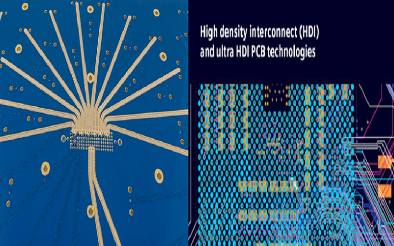
High Speed PCB Impedance: Core Fundamentals
Definition & Physical Basis
Characteristic impedance (Z₀) is the instantaneous impedance seen by a propagating signal traveling down a trace relative to its reference plane, defined by the ratio of trace inductance to capacitance per unit length.
- Impedance uniformity: ±5% tolerance mandated by IPC-2221 for signals ≥1Gbps.
- Transmission line behavior activates when trace length exceeds λ/10, where λ represents signal wavelength.
- Impedance mismatch >10% generates >20% signal reflection, causing eye closure and bit errors.
Impedance vs Frequency Stability
- Low Loss PCB maintains impedance stability within ±2% from 1–10GHz.
- ultra low loss pcb delivers ±1% stability up to 50GHz, ideal for 50Gbps+ interfaces.
- hdi pcb structures demand tighter impedance control due to reduced dielectric thickness and finer features.
Key Aspects of High-Speed PCB Impedance
Controlled Impedance
Controlled impedance ensures consistent Z₀ along entire trace lengths through fixed trace width, dielectric height, and material selection.
- Mandatory for PCIe, Ethernet, USB 3.x, DDR, and RF interfaces.
- Impedance tolerance: ±5% standard; ±3% for ultra low loss pcb operating ≥25Gbps.
- Impedance test coupons required on production panels per IPC-6012 Class 3.
Signal Reflection
Reflection occurs when impedance discontinuities disrupt wave propagation, quantified by reflection coefficient (Γ).
- Γ = (Zₗₒₐ𝒹 – Z₀) / (Zₗₒₐ𝒹 + Z₀)
- Reflections >-15dB violate IPC-2221 limits for high speed pcb.
- Stub resonations at ¼ wavelength create worst-case reflections.
Design Factors Determining Trace Impedance
Physical Trace Parameters
- Trace width (W): Directly inversely proportional to impedance; ±0.5mil variation changes Z₀ by ±3–5Ω.
- Trace thickness (T): 1oz (35μm) or 2oz (70μm) copper; thicker copper lowers impedance by 2–4Ω.
- Dielectric height (H): Distance from trace to reference plane; dominant factor influencing impedance.
- Trace profile: Trapezoidal etching reduces effective width by 0.2–0.3mil, altering impedance.
Material Properties
- Dielectric constant (Dk/εᵣ): FR-4 = 4.2–4.7; Low Loss PCB = 3.7–4.0; ultra low loss pcb = 3.0–3.5.
- Dissipation factor (Df): Lower values preserve signal power and impedance stability.
- Glass weave effect: Causes impedance variation ±4Ω in standard materials; minimized in Low Loss PCB.
Impedance Calculation Models & Formulas
Microstrip Impedance (Outer Layer)
Single-ended microstrip formula (industry-standard IPC-2221):
Z₀ = (87 / √(Dk + 1.41)) × ln(5.98×H/(0.8×W + T))
- Valid for W:H ratios between 0.1 and 2.0.
- Example: 4mil width, 8mil dielectric, Dk=4.0, 1oz copper → 50.2Ω.
Stripline Impedance (Inner Layer)
Symmetric stripline formula:
Z₀ = (60 / √Dk) × ln(1.9×H/(0.8×W + T))
- Centered trace between two parallel reference planes.
- Example: 4mil width, 8mil total dielectric, Dk=4.0 → 48.7Ω.
Differential Impedance
Differential impedance (Z𝒹𝒾𝒻𝒻) = 2×Z₀×(1–0.48×exp(-0.96×S/H))
- S = spacing between paired traces.
- 100Ω differential pairs use ~50Ω single-ended traces with tight spacing.
Learn more about: 50Ω / 75Ω / 100Ω Impedance in High Density Interconnect (HDI) PCBs: Design & Production Guide
Common Target Impedances
Single-Ended Signals
- 50Ω: RF, high-speed logic, DDR, general high speed pcb signals.
- 75Ω: Video, coax-compatible interfaces.
- 60Ω: Some memory interfaces, custom analog circuits.
Differential Pairs
- 90Ω: USB 3.0/3.1/3.2.
- 100Ω: PCIe 1–6, Ethernet 10/40/100/400G, HDMI 2.0/2.1.
- 85Ω: DDR5 differential DQ signals.
Commonly Used High Frequency PCB Materials
Material Comparison Table
| Material Type | Dk @10GHz | Df @10GHz | Best For | Impedance Stability |
|---|---|---|---|---|
| Standard FR-4 | 4.3–4.7 | 0.018–0.025 | ≤5Gbps | ±4–6Ω |
| Low Loss PCB | 3.7–4.0 | 0.004–0.009 | 5–25Gbps | ±2–3Ω |
| ultra low loss pcb | 3.0–3.5 | 0.0015–0.003 | ≥25Gbps | ±1–2Ω |
| hdi pcb Laminate | 3.6–3.9 | 0.005–0.008 | Fine-pitch BGA | ±2Ω |
Learn more about: High-Speed PCB Materials: A Complete Comparison Guide
Manufacturing Impact
- Prepreg flow variation changes dielectric height by ±10%, shifting impedance ±4–6Ω.
- Low Loss PCB offers tighter resin distribution for consistent impedance.
- ultra low loss pcb uses spread glass technology to minimize impedance variation.
Routing Guidelines for Impedance Control
Trace Routing Rules
- Maintain constant width; avoid necking longer than 2x width.
- Use 45° or curved bends; 90° bends increase impedance by 5–8Ω.
- Pair spacing fixed along entire differential pair length.
Reference Plane Rules
- Solid, continuous reference planes; gaps >50mil cause >10Ω impedance shift.
- 20H rule: Power planes inset 20× dielectric thickness from ground planes.
- Route high speed traces over solid planes only; avoid plane splits.
Termination & Impedance Matching
Termination Methods
- Series termination: 30–50Ω resistor at driver source.
- Parallel termination: 50–100Ω resistor at load end.
- AC termination: Series capacitor + resistor across differential pair.
Matching Standards
- Match impedance to within ±5% for eye opening >30% at 25Gbps.
- Back-drilling eliminates via stubs >5mil, preserving impedance.
- hdi pcb uses microvias to avoid stub-related discontinuities.
Case Study: 12-Layer HDI Ultra Low Loss PCB
Project Specifications
- Layers: 12-layer symmetric stackup; signal layers 1,3,10,12.
- Data rate: 50Gbps NRZ; impedance targets: 50Ω SE, 100Ω differential.
- Material: ultra low loss pcb (Dk=3.2, Df=0.002); dielectric height: 4.7mil.
- Trace specs: 4.0mil width, 4.8mil spacing, 1oz copper.
Issues Encountered
- Initial impedance: 56Ω (12% high) due to incorrect dielectric height.
- Differential pair skew caused impedance mismatch >8Ω.
- Plane gaps created 10Ω impedance variation along trace length.
Improvements Implemented
- Adjusted trace width to 4.5mil; corrected dielectric to 4.2mil.
- Restacked to symmetric layer arrangement; eliminated plane gaps.
- Implemented length matching ±1mil and fixed pair spacing.
Results
- Final impedance: 50.1Ω SE, 99.7Ω differential (±0.5% tolerance).
- Return loss improved from -8dB to -22dB.
- Manufacturing yield increased from 79% to 96.8%.
| Case Study Aspect | Details |
|---|---|
| Project Specs | 12-layer HDI, 50Gbps, ultra low loss pcb, Dk=3.2, 4.0mil trace, 4.8mil space |
| Issues | Impedance 12% high, 8Ω mismatch, plane gap variation |
| Fixes | 4.5mil trace, 4.2mil dielectric, symmetric stack, solid planes |
| Results | 50.1Ω / 99.7Ω, -22dB return loss, yield 96.8% |
Common Design Errors
- Incorrect Trace Width: Using 4mil instead of 4.5mil creates 6Ω impedance shift requiring full redesign.
- Plane Discontinuities: Routing over gaps or slots changes impedance by 8–12Ω, causing rejections.
- Material Specification Errors: Substituting standard FR-4 for Low Loss PCB increases variation by 200%.
- Neglecting Etch Compensation: Trapezoidal trace shape causes 3–5Ω uncompensated shift.
Quality Control & Compliance
Testing Protocols
- TDR measurement: 50ps rise time; impedance tested at 8 points per coupon.
- Impedance coupon: 12-inch trace length placed on panel edges.
- X-section inspection: Verify dielectric height and trace geometry.
Standards Compliance
- IPC-2221: Generic standard for impedance design.
- IPC-6012: Qualification and performance specification.
- IPC-TM-650: Test method for TDR impedance measurement.
FAQ
Q1: What’s the difference between microstrip and stripline impedance?
A1: Microstrip (outer layers) uses one reference plane and is easier to manufacture; stripline (inner layers) uses two planes for 35% better noise immunity and consistent impedance. Low Loss PCB improves stripline stability by 30% over FR-4.
Q2: How does Dk value affect high speed pcb impedance calculation?
A2: Dk is inversely proportional to impedance; higher Dk reduces Z₀. Standard FR-4 (Dk=4.5) yields lower impedance than ultra low loss pcb (Dk=3.2) with identical geometry. A 0.3 Dk shift changes impedance by ~4Ω.
Q3: What trace tolerance is required for ±5% impedance control?
A3: Trace width must hold ±0.3mil; dielectric height ±0.2mil. hdi pcb requires ±0.2mil trace tolerance for ±3% impedance stability, standard in advanced PCB fabrication.
Q4: How to compensate for impedance variation in mass production?
A4: Use impedance coupons on every panel; adjust trace width ±0.1–0.2mil based on TDR feedback. Low Loss PCB reduces production variation by 50% compared to standard FR-4.
If you need professional high speed PCB impedance design support or quotation, our team provides free DFM check and fast turnaround.


![Understanding PCB Costs & Pricing [Your Complete Guide]](https://hdicircuitboard.com/wp-content/uploads/elementor/thumbs/Understanding-PCB-Costs-Pricing-Your-Complete-Guide-qzzhe6mcaxuolkux3xalfktgavumi9y1aqfbs9bpv4.webp "Understanding PCB Costs & Pricing [Your Complete Guide]")


