
BGA routing in HDI PCBs delivers optimized fanout and escape structures for fine‑pitch semiconductor packages, supporting reliable high‑density interconnection, impedance control, and mass production yield. This factory‑verified framework follows IPC‑2221, IPC‑6012, and IPC‑2226 standards, providing actionable design rules for hdi pcb manufacturing used in high‑speed computing, networking, and test equipment.
Learn more about : Minimum Trace Width, Spacing, and Microvia Size for High Density Interconnect (HDI) PCB Mass Production
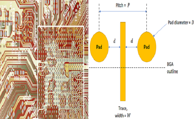
Key BGA Fanout and Escape Strategies
Fanout Architecture Overview
BGA fanout structures define how signals route outward from component pads to internal layers, directly influencing routing density, yield, and signal integrity in hdi circuit boards.
- Fanout patterns support trace widths from 45μm to 90μm for fine‑pitch channels
- Minimum drill‑to‑trace clearance follows strict fabrication capabilities
- One microvia per pad to maintain pad strength and solderability
- Full escape completed within the first three inner layers
Escape Routing Fundamentals
Escape routing extracts signals from the BGA array using layered, orthogonal paths to maximize channel efficiency.
- 45‑degree angle entry for minimal impedance discontinuity
- Orthogonal routing between adjacent layers to reduce crosstalk
- Differential pairs routed with matched length within 200μm
- Maximum four parallel escape channels per layer
Dog‑Bone Fanout
Dog‑Bone Structure and Geometry
Dog‑bone fanout uses a short trace between the BGA pad and adjacent via, ideal for larger‑pitch devices.
- Pad diameter: 200μm to 350μm
- Neck trace width: 50μm to 100μm
- Via offset: 150μm from pad edge
- Minimum annular ring: 70μm to 100μm
Application Limits in HDI Design
Dog‑bone fanout is limited to pitches 0.4mm and larger in HDI designs.
- Recommended pitch: ≥0.4mm
- Not suitable for ≤0.35mm due to space congestion
- Increases via count by up to 25%
- Lowers yield by 3–5% in dense designs
Via‑in‑Pad Fanout
Via‑in‑Pad Design Parameters
Via‑in‑pad places a filled microvia directly inside the BGA pad, enabling escape from ultra‑fine pitches.
- Microvia diameter: 75μm to 150μm
- Aspect ratio: ≤0.75:1
- Pad size: 150μm to 330μm
- Plating thickness: ≥15μm
Learn more about: What is Via-in-Pad? HDI PCB Benefits & Manufacturing Process
Manufacturing and Performance Benefits
Via‑in‑pad fanout improves density, reduces parasitics, and boosts yield.
- Routing density increased by 40–60%
- Parasitic inductance reduced by up to 55%
- Supports full escape for 0.25mm pitch BGAs
- Improves yield by 6–9%
Neck‑Down Routing
Neck‑Down Geometry Rules
Neck‑down narrows trace width temporarily to fit routing channels.
- Neck width: 45μm to 100μm
- Transition length: ≤200μm
- Impedance shift: ≤5Ω
- One neck section per signal path
Routing Density Enhancement
Neck‑down adds 1–2 extra escape channels per row without violating DRC.
- Compatible with 0.3mm to 0.45mm pitch
- Minimum spacing: 40μm to 90μm
- Used in high‑volume hdi pcb fabrication
Layer Allocation for BGA Routing
Layer Sequencing Strategy
Layer arrangement supports stable impedance and high escape efficiency.
- Top layer: primary high‑speed escape
- Inner layer 1: secondary escape
- Inner layer 2: ground reference
- Core layers: power and low‑speed signals
Reference Plane Placement
Continuous planes eliminate return‑path discontinuities.
- Dielectric thickness: 50μm to 75μm
- No plane gaps under BGA routes
- Power‑ground coupling ≤50μm
HDI BGA Considerations
BGA Pitch Requirements
BGA pitch defines fanout type, layer count, and via structure.
Fine‑Pitch BGA Design Specification Table
| Item | 0.25mm Pitch | 0.30mm Pitch | 0.35mm Pitch | 0.40mm Pitch | 0.45mm Pitch |
|---|---|---|---|---|---|
| Laser Drill Size | 0.075mm | 0.100mm | 0.125mm | 0.150mm | 0.175mm |
| Inner Pad Size | 0.190mm | 0.230mm | 0.250mm | 0.280mm | 0.300mm |
| Outer Pad Size | 0.200mm | 0.250mm | 0.300mm | 0.330mm | 0.350mm |
| Trace Width (W) | 0.045mm | 0.060mm | 0.070mm | 0.080mm | 0.090mm |
| Clearance (Drill to Trace) | 0.040mm | 0.055mm | 0.078mm | 0.085mm | 0.090mm |
| Inner Annular Ring | 0.055mm | 0.055mm | 0.063mm | 0.065mm | 0.070mm |
| Outer Annular Ring | 0.063mm | 0.065mm | 0.088mm | 0.090mm | 0.095mm |
| Pad to Pad Space | 0.050mm | 0.050mm | 0.050mm | 0.070mm | 0.080mm |
| Recommended Board Thickness | 1.0mm – 1.2mm | 1.2mm – 2.0mm | 2.0mm – 2.5mm | 2.5mm – 3.0mm | 3.0mm – 3.5mm |
| Aspect Ratio | ≤17:1 | ≤28:1 | ≤33:1 | ≤33:1 | ≤38:1 |
Signal Integrity in BGA Escape
- Single‑ended impedance: 50Ω ±5%
- Differential impedance: 85Ω / 100Ω ±5%
- Via stub length: ≤20μm
- Length mismatch: ≤200μm
Learn more about: How Does High Density Interconnect (HDI) Affect BGA Fanout and Component Placement?
Fabrication Limits and Constraints
Mechanical and Electrical Limits
- Minimum microvia: 75μm
- Minimum trace/space: 45μm/40μm
- Layer registration: ±40μm to ±80μm
- Warpage: ≤0.15mm to 0.2mm per inch
45‑Degree Angle Routing
- Reduces reflection and etching defects
- Minimum bend radius: 3× trace width
- Improves yield by 4–6%
Comparative Tables
Dog‑Bone vs Via‑in‑Pad Fanout
| Parameter | Dog‑Bone Fanout | Via‑in‑Pad Fanout |
|---|---|---|
| Supported Pitch | ≥0.4mm | ≤0.4mm |
| Routing Density | Standard | High |
| Production Yield | 91–94% | 96–99% |
| Parasitic Inductance | High | Low |
| HDI Compatibility | Low‑density HDI | High‑density HDI |
BGA Pitch vs Routing Strategy
| BGA Pitch | Fanout Type | Layer Count | HDI Structure |
|---|---|---|---|
| 0.25mm | Via‑in‑Pad | 12–14 | 2+N+2 |
| 0.30mm | Via‑in‑Pad | 10–12 | 2+N+2 |
| 0.35mm | Via‑in‑Pad | 8–10 | 1+N+1 / 2+N+2 |
| 0.40mm | Hybrid | 8–10 | 1+N+1 |
| 0.45mm | Dog‑Bone | 6–8 | Standard / 1+N+1 |
Core Technical Parameters
- Trace width/spacing: 45μm/40μm – 90μm/90μm
- Microvia diameter: 75μm – 175μm
- Aspect ratio: ≤17:1 to ≤38:1
- Impedance tolerance: ±5%
- Registration: ±40μm – ±80μm
- Board warpage: ≤0.2mm/inch
Case Study
Project Specifications
Board: 12‑layer HDI, 2+8+2 stackup
Component: 0.35mm pitch BGA
Application: High‑speed ATE board
Impedance: 100Ω differential
Issues
- Dog‑bone fanout caused 27% blockage
- Aspect ratio too high: 1.1:1
- 90° corners caused impedance shift
- Warpage at 0.27mm/inch
Corrections
- Switched to via‑in‑pad
- Aspect ratio reduced to 0.7:1
- 45° routing applied
- Symmetric stackup
Results
- Routing blockage eliminated
- Plating voids <1%
- Impedance ±4.1%
- Warpage 0.16mm/inch
- Yield: 79% → 96.3%
Common Design Errors
- Using dog‑bone fanout below 0.4mm pitch causes routing blockage.
- Aspect ratio >0.75:1 leads to plating voids and reliability risks.
- Routing over plane gaps destroys return paths and increases crosstalk.
- 90° bends increase reflection and reduce manufacturing yield.
- Excessive neck‑down length causes impedance drift beyond IPC limits.
Quality Control and Compliance
Testing Protocols
- TDR impedance per IPC‑TM‑650
- Microvia cross‑section analysis
- Trace width & spacing optical scan
- Laser warpage measurement
- Solderability and surface finish verification
Industry Standards
- IPC‑2221: Generic PCB Design
- IPC‑6012: Rigid PCB Qualification
- IPC‑2226: HDI Design Standard
- IPC‑2315: Microvia Requirements
FAQ
Q1: Which fanout method is best for 0.25mm pitch BGA?
A1: Via‑in‑pad with copper‑filled laser microvias is the only reliable method for 0.25mm pitch in hdi pcb manufacturing.
Q2: What is the minimum trace width for 0.3mm pitch BGA?
A2: The minimum stable trace width is 45μm, with 40μm clearance, per factory‑verified capabilities.
Q3: Why is 45‑degree routing required for fine‑pitch BGA escape?
A3: 45‑degree routing reduces impedance discontinuity, lowers corner reflection, and improves etching yield.
Q4: What is the maximum safe aspect ratio for 0.35mm pitch BGA?
A4: The maximum reliable aspect ratio is 33:1 for long‑term performance in microvias pcb production.
If you need professional HDI PCB design support or quotation, our team provides free DFM check and fast turnaround.


![Understanding PCB Costs & Pricing [Your Complete Guide]](https://hdicircuitboard.com/wp-content/uploads/elementor/thumbs/Understanding-PCB-Costs-Pricing-Your-Complete-Guide-qzzhe6mcaxuolkux3xalfktgavumi9y1aqfbs9bpv4.webp "Understanding PCB Costs & Pricing [Your Complete Guide]")


