
Signal integrity challenges in HDI PCBs arise from miniaturized geometries, high-density routing, and high-speed signaling, creating issues including impedance mismatch, crosstalk, return path disruptions, and attenuation. This factory-verified analysis quantifies electrical risks, provides mitigation frameworks, and aligns with IPC‑2221, IPC‑2226, and IPC‑6016 standards to ensure reliable transmission in hdi pcb manufacturing.
Learn more about: Power Integrity & PDN Design for High Speed PCBs
What is PCB Signal Integrity
Signal integrity defines the ability of electrical signals to propagate across interconnects without distortion, reflection, or noise interference. In HDI circuits, signal integrity directly determines system stability, data rate support, and long‑term reliability.
Core Electrical Definitions
- Signal distortion: waveform deformation caused by impedance variation or interference
- Return path: low‑inductance route for current to complete its circuit loop
- Transmission line effect: trace behavior as controlled impedance at rise times below 1ns
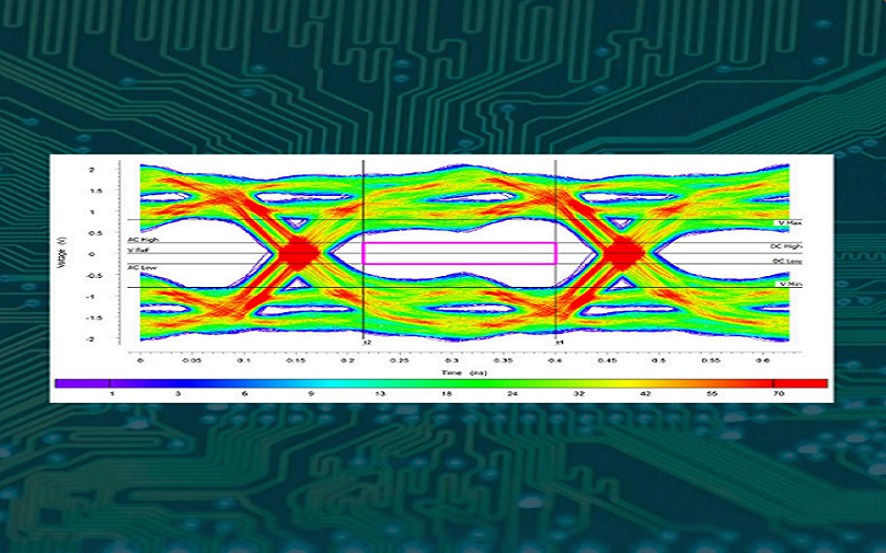
- Eye diagram closure: visual measure of signal quality and noise margin
Signal Integrity in HDI Context
HDI structures amplify signal integrity risks due to fine traces, tight spacing, and microvia transitions.
- Trace density increases by 40–60% compared to standard PCBs
- Microvia parasitics reduce stub length but introduce capacitive effects
- High‑speed data rates reach 112Gbps PAM4 and above
- Thinner dielectrics strengthen coupling but raise crosstalk risks
Major Signal Integrity Challenges in HDI PCBs
Impedance Mismatches & Reflections
Impedance discontinuities create signal reflections that degrade waveform quality and increase bit error rates.
- Trace width tolerance: ±8μm etch shift causes ±5% impedance change
- Via stub resonance: stub length over 20μm induces reflection peaks
- Layer transition mismatch: via pad and anti‑pad geometry disrupt impedance
- Target compliance: 50Ω single‑ended ±5%; 100Ω differential ±5% per IPC‑2221
Crosstalk
Aggressive routing density elevates coupling between adjacent traces, corrupting adjacent signals.
- Near‑end crosstalk (NEXT): coupling from parallel routing sections
- Far‑end crosstalk (FEXT): cumulative coupling along trace length
- 3W rule: spacing equal to 3× trace width reduces crosstalk by 70%
- Orthogonal layer routing: cancels electric field overlap between layers
Return Path Discontinuities
Gaps or splits in reference planes force long return paths, increasing loop inductance and EMI.
- Plane gaps under differential pairs: increase skew by 10–20ps
- Via anti‑pad clearance: excessive clearance breaks continuous return path
- Ground plane consistency: solid planes reduce inductance by 40%
- Return path length: controlled below 0.5mm for high‑speed channels
Signal Skew
Skew occurs when paired signals arrive at different times, degrading differential performance.
- Length mismatch: maximum 200μm for differential pairs
- Dielectric variation: Dk tolerance ±0.05 causes velocity mismatch
- Via count imbalance: unequal via count adds 5–10ps delay per via
- Skew limit: ≤5ps for 112Gbps PAM4 channels
Attenuation and Loss
Copper and dielectric losses increase exponentially at high frequencies, reducing signal amplitude.
- Insertion loss: ≤0.58dB at 50GHz for reliable transmission
- Dielectric loss: Df ≤0.007 for ultra‑high‑speed designs
- Copper roughness: Rz ≤1.5μm reduces skin effect loss
- Trace length: limited to ≤50mm for 56Gbps+ channels
Thermal Management & Noise
Temperature gradients alter dielectric properties and induce impedance drift.
- Tg ≥170°C maintains stability at reflow temperatures
- Thermal expansion: CTE z‑axis ≤3.5% minimizes dimensional shift
- Thermal vias: 100–200 vias per square inch for heat dissipation
- Impedance drift: ≤3% across operating temperature range
Parasitic Capacitance and Inductance
Microvias and fine traces introduce unintended reactive components.
- Microvia inductance: 0.5–0.8nH per via
- Trace inductance: 7–10nH/cm for 75μm traces
- Parasitic capacitance: 0.8–1.2pF per via
- Stacked vias: increase parasitics by 15–25%
Learn more about: Signal Integrity in High Speed PCB: Problems & Fixes
Mitigation Strategies for HDI Signal Integrity
Controlled Impedance Routing
Precision trace geometry stabilizes impedance across transmission lines.
- Field solver calculation: 2D/3D simulation for trace width optimization
- Microstrip vs stripline: stripline reduces noise by 25–35%
- 45‑degree routing: eliminates corner discontinuities
- Bend radius: minimum 3× trace width
Strategic Layer Stacking
Symmetric stackups eliminate warpage and stabilize impedance.
- 2+N+2 structure: dual build‑up layers for 56–112Gbps
- Reference plane pairing: signal layers nested between ground planes
- Dielectric thickness: 40–75μm for tight coupling
- Symmetric layer order: warpage ≤0.2mm/m
Using Advanced Materials
Low‑loss materials reduce high‑frequency attenuation.
- Low‑loss dielectric: Df ≤0.009 for 56Gbps; ≤0.007 for 112Gbps
- High‑Tg laminates: Tg ≥170°C for thermal stability
- Low‑profile copper: Rz ≤1.5μm for reduced loss
- Halogen‑free options: compliant with environmental standards
Learn more about: High-Speed PCB Materials: A Complete Comparison Guide
Ground Stitching Vias
Stitching vias stabilize reference planes and reduce EMI.
- Pitch: ≤1mm along differential pair guard traces
- Diameter: 100–150μm for low inductance
- Placement: within 0.3mm of signal vias
- Array density: 4–6 vias per mm for high‑speed sections
Design for Manufacturability
Design rules aligned with fabrication capabilities eliminate yield risks.
- Microvia aspect ratio: ≤0.75:1 for reliable plating
- Trace/space: 75μm/75μm minimum for mass production
- Registration tolerance: ±25μm layer‑to‑layer
- Annular ring: ≥50μm for microvia reliability
High-Speed Digital PCB Materials
Material selection directly impacts insertion loss and impedance stability.
- Standard FR‑4: Df 0.015–0.020 for low‑speed circuits
- Mid‑loss: Df 0.009–0.012 for 56Gbps systems
- Ultra‑low‑loss: Df ≤0.007 for 112Gbps+ links
- Copper weight: 12μm for signal layers; 35μm for power planes
Comparative Tables
Microstrip vs Stripline Signal Integrity Performance
| Structure | Impedance Stability | EMI Resistance | Loss Level |
|---|---|---|---|
| Microstrip | Good | Moderate | Medium |
| Stripline | Excellent | Excellent | Low |
Material Type vs High-Speed Loss Performance
| Material Category | Df Range | Max Data Rate | Application |
|---|---|---|---|
| Standard FR-4 | 0.015–0.020 | ≤28Gbps | Consumer |
| Mid-Loss | 0.009–0.012 | 56Gbps | Networking |
| Ultra-Low-Loss | ≤0.007 | 112Gbps+ | Computing |
Core Technical Specifications
- Layer count: 4–40 layers
- Board thickness: 0.40–7.60mm
- Trace/space: 50μm/50μm inner; 75μm/75μm outer
- Microvia diameter: 75μm
- Aspect ratio: ≤0.75:1
- Impedance tolerance: ±5%
- Dielectric thickness: 40–75μm
- Registration: ±25μm
- Warpage: ≤0.2mm/m
- Insertion loss: ≤0.58dB@50GHz
Case Study
Project Overview
Board type: 12‑layer 2+8+2 HDI PCB; Application: 800G optical module; BGA pitch: 0.65mm; Impedance: 100Ω differential.
Issues Encountered
Asymmetric stackup caused 0.27mm/m warpage; microvia aspect ratio 1.1:1 created plating voids; 90‑degree bends induced reflections; insertion loss exceeded 1.1dB at 50GHz.
Corrective Actions
Symmetric stackup implemented; aspect ratio reduced to 0.7:1; 45‑degree routing applied; ultra‑low‑loss Df ≤0.007 material used.
Final Results
Impedance controlled to ±4.1%; warpage stabilized at 0.16mm/m; insertion loss ≤0.58dB@50GHz; yield improved from 79% to 96.3%.
Common Design Errors
- Asymmetric stackups induce warpage exceeding 0.25mm/m and break impedance consistency.
- Microvia aspect ratio >0.75:1 causes plating voids and parasitic impedance shifts.
- Reference plane gaps under high‑speed traces disrupt return paths and increase crosstalk.
- 90‑degree trace angles create impedance discontinuities and signal reflection.
- Ignoring copper roughness in simulation leads to underestimated insertion loss.
Quality Control & Compliance
Testing Protocols
- TDR impedance measurement per IPC‑TM‑650
- Insertion/return loss testing up to 50GHz
- Microvia cross‑section analysis for void detection
- Thermal cycling: –40°C to 125°C, 1000 cycles
- Laser warpage profiling
Industry Standards
- IPC‑2221: Generic PCB design standard
- IPC‑2226: HDI design requirements
- IPC‑6012: Rigid PCB performance
- IPC‑6016: HDI acceptance criteria
- ISO 9001, IATF 16949, UL, RoHS
Frequently Asked Questions
Q1: What impedance tolerance is required for high-speed HDI PCBs?
A1: Industry and IPC standards require ±5% impedance tolerance for single‑ended and differential channels in hdi pcb fabrication.
Q2: Which stackup structure best supports signal integrity in HDI designs?
A2: Symmetric 2+N+2 HDI stackups provide optimal impedance stability and noise performance for 56–112Gbps applications.
Q3: How does material loss affect signal integrity in HDI PCBs?
A3: Lower dissipation factor (Df) reduces high‑frequency attenuation; Df ≤0.007 is required for 112Gbps+ systems.
Q4: What is the maximum safe via stub length for high-speed HDI signals?
A4: Via stub length must be ≤20μm to avoid resonance and signal distortion in microvias pcb high‑speed channels.
If you need professional HDI PCB design support or quotation, our team provides free DFM check and fast turnaround.


![Understanding PCB Costs & Pricing [Your Complete Guide]](https://hdicircuitboard.com/wp-content/uploads/elementor/thumbs/Understanding-PCB-Costs-Pricing-Your-Complete-Guide-qzzhe6mcaxuolkux3xalfktgavumi9y1aqfbs9bpv4.webp "Understanding PCB Costs & Pricing [Your Complete Guide]")


