
Via-in-Pad (VIPPO) technology places plated microvias directly within component pads in HDI PCBs, enabling higher routing density, shorter electrical paths, and improved thermal performance while eliminating solder wicking risks through controlled filling and plating processes. This implementation follows IPC‑2221, IPC‑2226, and IPC‑6016 standards and supports fine‑pitch BGAs, advanced processors, and miniaturized assemblies used in consumer, automotive, and medical electronics.
Learn more about: What is Via-in-Pad? HDI PCB Benefits & Manufacturing Process
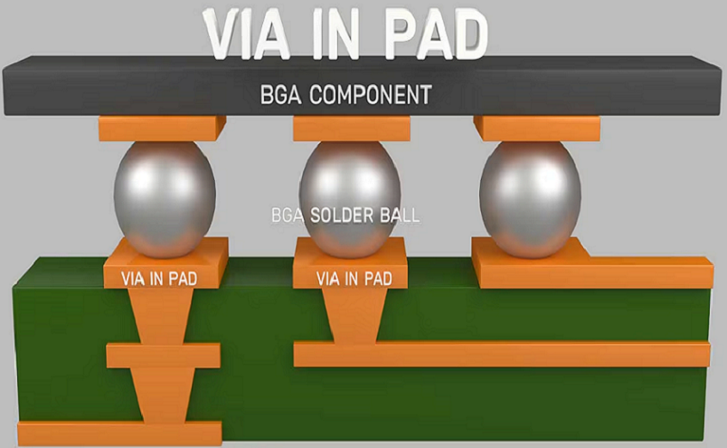
What is Via-in-Pad in HDI PCB Design
Via-in-Pad refers to a high-density interconnect technique where a laser‑drilled microvia is positioned inside a surface mount pad rather than in the surrounding clearance area. The via is typically filled with conductive or non‑conductive epoxy and plated over to create a flat, solderable surface.
Definition and Core Function
- Places microvias directly within SMD pads to maximize routing space
- Eliminates the need for fanout routing outside component footprints
- Reduces stub length and improves signal integrity in high‑speed designs
- Supports 0.3mm to 0.65mm fine‑pitch BGA components
VIPPO vs. Conventional Fanout
VIPPO (Via-in-Pad Plated Over) creates a flush surface ideal for assembly, while traditional fanout routes traces away from pads with external vias. This distinction defines routing efficiency, yield, and high‑speed behavior in hdi pcb manufacturing.
Learn more about: BGA Routing in HDI PCBs: Fanout & Escape Techniques
Key Advantages of Via-in-Pad in HDI Designs
Space Savings and Routing Density
Via-in-Pad increases routing efficiency by up to 60% compared to conventional fanout.
- Eliminates clearance areas required for off-pad vias
- Supports two to three escape rows under fine‑pitch BGAs
- Reduces overall layer count by 20–30% in complex designs
- Minimum trace/space reduced to 50μm/50μm in inner layers
Electrical and Thermal Performance
Shortened electrical paths lower parasitic inductance and improve thermal dissipation.
- Via stub length limited to ≤20μm for minimal signal reflection
- Parasitic inductance reduced by 30–50% compared to through vias
- Thermal resistance lowered by 25–40% for high‑power components
- Supports 56Gbps and 112Gbps high‑speed signaling with stable impedance
Manufacturing Process: VIPPO Production Flow
Laser Drilling and Metallization
Microvias are formed using UV laser drilling followed by desmear and metallization.
- Laser drill diameter: 75μm to 125μm for HDI applications
- Aspect ratio controlled to ≤0.75:1 for reliable plating
- Copper plating thickness: 15–25μm for structural integrity
- Registration accuracy: ±20μm layer‑to‑layer
Filling and Plating Over
The via filling process ensures a flat surface for reliable soldering.
- Non-conductive epoxy filling for standard applications
- Conductive paste filling for enhanced thermal performance
- Vacuum filling to eliminate voids (<1% void allowance per IPC‑6016)
- CMP planarization for ≤5μm surface planarity
Key Challenges and Limitations
Manufacturing Complexity and Cost
Via-in-Pad requires specialized equipment and tighter process control.
- Production cost increases by 15–30% compared to standard vias
- Requires laser drilling, vacuum filling, and planarization steps
- Yield sensitivity increases with miniaturized geometries
- Etching and plating control must maintain ±8μm trace accuracy
Assembly and Reliability Risks
Improper filling leads to solder voids, head-in-pillow defects, and early failures.
- Solder wicking if filling is incomplete or non‑planar
- Thermal stress concentration at rigid‑flex transitions
- Risk of delamination under high‑temperature reflow
- Microcracking in filled vias under temperature cycling
Common Applications of Via-in-Pad
High-Density Component Escape
Via-in-Pad enables effective routing from ultra‑fine‑pitch packages.
- 0.3mm–0.65mm pitch BGAs in mobile and wearable devices
- High‑performance processors, FPGAs, and SerDes chips
- RF transceivers and high‑speed analog frontends
- Miniaturized medical sensors and implantable devices
High-Speed and Thermal Designs
The structure supports demanding electrical and thermal environments.
- 56Gbps and 112Gbps PAM4 communication links
- Automotive ADAS controllers and power management ICs
- High‑power LED and RF amplifier thermal paths
- Impedance‑controlled transmission lines in microvias pcb structures
Critical Design Rules for Via-in-Pad
Drill-to-Copper Clearance and Annular Ring
Strict geometric controls ensure plating reliability and electrical isolation.
- Minimum annular ring: 50μm for laser microvias
- Drill-to-copper clearance: ≥75μm on inner layers
- Via diameter range: 75μm–125μm for production stability
- Anti‑pad size optimized to avoid return path disruption
Material and Stackup Constraints
Material selection directly impacts plating, filling, and reliability.
- Dielectric thickness: 40–75μm for HDI build‑up layers
- High‑Tg resins (Tg ≥170°C) for reflow stability
- Low CTE materials to reduce thermal stress
- Stackup types: 1+N+1 and 2+N+2 for optimal VIPPO performance
Alternative Techniques to Via-in-Pad
Dog-Bone Fanout
A lower-cost alternative for less dense components.
- Suitable for pitch ≥1.0mm BGAs
- Lower manufacturing cost and complexity
- Larger routing area required
- Higher parasitic inductance and signal loss
Offset Via Fanout
Balances density and complexity for mid‑range designs.
- Works for 0.65mm–0.8mm pitch components
- Moderate space efficiency
- Reduced assembly risk compared to VIPPO
- Easier manufacturing tolerance control
Comparative Tables
Via-in-Pad vs. Dog-Bone Fanout Comparison
| Feature | Via-in-Pad (VIPPO) | Dog-Bone Fanout |
|---|---|---|
| Routing Density | Excellent | Moderate |
| Signal Integrity | Excellent | Good |
| Manufacturing Cost | High | Low |
| Suitable Pitch | ≤0.65mm | ≥1.0mm |
| Assembly Risk | Low (when filled) | Very Low |
Microvia vs. Through-Hole Via Performance
| Parameter | Laser Microvia (VIPPO) | Through-Hole Via |
|---|---|---|
| Aspect Ratio | ≤0.75:1 | Up to 10:1 |
| Parasitic Inductance | Low | High |
| Stub Length | ≤20μm | Full board thickness |
| High-Speed Suitability | Excellent | Poor |
Core Technical Specifications
- Minimum microvia diameter: 75μm
- Aspect ratio: ≤0.75:1
- Trace/space capability: 50μm/50μm
- Annular ring: 50μm minimum
- Void allowance: <1% in filled vias
- Surface planarity: ≤5μm
- Impedance tolerance: ±5% per IPC‑2221
- Operating temperature: -40°C to 125°C
- Compliance: IPC‑2226, IPC‑6016, IPC‑6012
Case Study
Project Overview
Board type: 10‑layer 2+6+2 HDI PCB; BGA pitch: 0.5mm; Impedance target: 100Ω differential; Application: 800G optical module.
Issues Encountered
Initial design used offset vias causing insufficient routing space; incomplete via filling led to solder wicking; impedance deviation reached ±9%; layer registration error hit 35μm.
Corrective Actions
Implemented VIPPO with vacuum epoxy filling; optimized annular ring to 60μm; tightened registration to ±20μm; adjusted trace width for ±4% impedance control.
Final Results
Routing completed within 8 layers instead of 10; solder defects eliminated; impedance stable at ±3.9%; production yield improved from 76% to 95.4%; full compliance with IPC‑6016 Class 3.
Common Design Errors
- Insufficient annular ring below 50μm causes plating fractures and open circuits.
- Missing via filling or non‑planar plating leads to solder wicking and BGA head-in-pillow defects.
- Aspect ratio exceeding 0.75:1 results in incomplete plating and reliability risks.
- Inadequate drill-to-copper clearance creates short circuits during etching.
- Ignoring stackup symmetry induces warpage and via cracking under thermal cycling.
Quality Control and Compliance
Factory Testing Protocols
- Microsection analysis for void detection and plating integrity
- CMM surface planarity measurement for filled vias
- Electrical open/short testing per IPC‑TM‑650
- Thermal shock testing: -40°C to 125°C, 100 cycles
- Impedance verification using TDR measurement
Industry Standards
- IPC‑2221: Generic PCB design standard
- IPC‑2226: HDI PCB design requirements
- IPC‑6016: HDI and microvia qualification
- IPC‑6012: Rigid PCB performance specification
- ISO 9001, IATF 16949, UL, RoHS
Frequently Asked Questions
Q1: What is the minimum pitch for reliable Via-in-Pad implementation?
A1: Via-in-Pad supports down to 0.5mm BGA pitch in mass production, with 0.3mm possible in advanced hdi pcb fabrication.
Q2: What is the standard void allowance for filled VIPPO structures?
A2: Industry and IPC standards allow less than 1% voiding in filled vias for Class 2 and Class 3 reliability.
Q3: Which stackup is most suitable for Via-in-Pad HDI designs?
A3: Symmetric 2+N+2 HDI stackups provide the best stability, registration, and impedance control for VIPPO.
Q4: What is the difference between conductive and non-conductive via filling?
A4: Conductive paste improves thermal performance, while non-conductive epoxy offers lower cost and sufficient electrical performance.
If you need professional HDI PCB design support or quotation, our team provides free DFM check and fast turnaround.


![Understanding PCB Costs & Pricing [Your Complete Guide]](https://hdicircuitboard.com/wp-content/uploads/elementor/thumbs/Understanding-PCB-Costs-Pricing-Your-Complete-Guide-qzzhe6mcaxuolkux3xalfktgavumi9y1aqfbs9bpv4.webp "Understanding PCB Costs & Pricing [Your Complete Guide]")


