
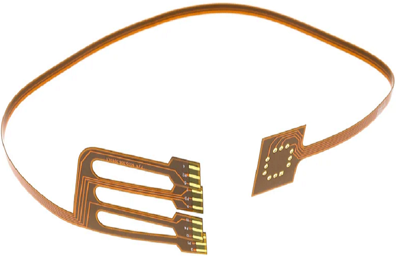
A flexible circuit board (FPC), also known as a flexible printed circuit board or bendable circuit board, is a thin, conformable interconnect solution constructed on flexible polymer dielectric materials, engineered to support static shaping, dynamic bending, and 3D assembly while maintaining consistent electrical performance. This guide delivers comprehensive engineering data, manufacturing specifications, design guidelines, and reliability standards aligned with IPC-2223, IPC-6013, and UL requirements, equipping beginners and designers with actionable insights for selecting, specifying, and validating flexible PCB solutions in production environments.
Learn more about: Flexible PCB: A Comprehensive Guide to Features, Applications, Types & Key Considerations
Definition and Core Characteristics
A flexible circuit board is an advanced electrical interconnect system built on flexible dielectric substrates that enables repeated bending, twisting, and installation into irregularly shaped enclosures. It replaces rigid FR-4 boards and traditional wiring harnesses with enhanced reliability, reduced volume, and greater mechanical flexibility.
- Base thickness ranges from 12.5μm to 125μm for pure flex structures
- Supports operating temperatures from -40°C up to 200°C
- Maintains electrical stability under continuous dynamic mechanical stress
- Reduces assembly complexity and interconnect failure points
- Complies with IPC-6013 for flexible and rigid-flex performance specifications
Fundamental Technical Principles
Flexible PCB technology operates on the principle of using ductile conductive materials and flexible dielectrics to maintain electrical integrity during mechanical deformation.
- Conductor materials feature high elongation rates (10-30%) to withstand bending without fracture
- Dielectric materials offer high tensile strength and tear resistance while maintaining electrical insulation
- Layer structures are engineered to distribute stress evenly during flexing operations
- Adhesive systems provide stable bonding between layers while retaining flexibility across temperature ranges
Distinguishing Characteristics from Rigid PCBs
Flexible circuit boards differ fundamentally from rigid PCBs in material composition, mechanical properties, and application suitability.
- Substrate materials: Flexible polyimide vs. rigid glass-reinforced epoxy (FR-4)
- Thickness: 50μm-125μm vs. 0.4mm-3.2mm for rigid boards
- Weight: 60-90% lighter than equivalent rigid interconnect solutions
- Installation capability: Conforms to curved surfaces vs. limited to flat mounting
- Dynamic performance: Withstands millions of bending cycles vs. susceptible to fracture under repeated flexing
Learn more about: What Is Flexible PCB
Key Advantages of Flexible Circuit Boards
Space Saving Optimization
Flexible PCBs deliver exceptional space efficiency through thin-profile design and 3D routing capabilities.
- Reduces assembly volume by up to 70% compared to traditional wiring harnesses
- Enables installation in irregular, constrained spaces impossible for rigid boards
- Supports component stacking and vertical integration through folding capabilities
- Eliminates required clearance for connectors by integrating interconnections directly
- Allows continuous routing around obstacles without connector interruptions
Weight Reduction Benefits
Weight savings represent one of the most significant advantages of flexible PCB technology.
- Achieves 60-90% weight reduction compared to conventional wiring assemblies
- Lowers overall product weight, critical for portable and aerospace applications
- Reduces structural support requirements and material costs
- Improves portability and battery life in mobile devices
- Decreases inertial forces in vibrating applications, enhancing reliability
Flexibility and Design Freedom
The inherent flexibility of these boards unlocks new design possibilities.
- Supports static bending for permanent shaping to fit enclosure contours
- Withstands dynamic bending for moving components (hinges, folds, slides)
- Enables innovative form factors and product designs
- Accommodates thermal expansion and contraction without stress fractures
- Allows design optimization for minimal space utilization
Enhanced Reliability Performance
Flexible circuits demonstrate superior reliability compared to traditional interconnect methods.
- Reduces connection points by 40-60%, minimizing potential failure sites
- Eliminates wire fatigue and crimp connection failures common in wiring harnesses
- Maintains performance under vibration, shock, and thermal cycling
- Resists corrosion and humidity better than conventional wiring
- Delivers consistent performance across -40°C to 150°C temperature ranges
Improved Thermal Management
Flexible PCB construction offers superior thermal dissipation characteristics.
- Thinner dielectric layers enable more efficient heat transfer
- Copper layers provide excellent thermal conductivity paths
- Direct contact with housing structures enhances heat dissipation
- Reduced thermal mass enables faster temperature stabilization
- Supports thinner heat sink requirements or eliminates them entirely
Exceptional Durability
Properly designed flexible circuits exhibit outstanding operational lifespan.
- Dynamic flexing life: 10,000 to 1,000,000+ cycles based on materials
- Resistance to flex fatigue compared to rigid boards and wiring
- Chemical resistance to solvents, oils, and environmental contaminants
- UV stability for outdoor and exposed applications
- Mechanical shock resistance exceeding 1,500G in optimized designs
Learn more about: What Is a Flexible Printed Circuit?
Common Applications of Flexible Circuits
Wearable Technology
Wearable devices represent ideal applications for flexible PCB technology.
- Smart watches and fitness trackers utilize 2-4 layer flex circuits
- Hearables and TWS earbuds use ultra-thin (25-50μm) single-sided flex
- Medical wearables employ biocompatible materials with 50μm line/space
- Flexible displays rely on specialized flex circuits with 1,000,000+ cycle endurance
- Smart textiles integrate flexible circuits directly into fabric substrates
Medical Devices
Medical applications demand the highest reliability and precision from flexible circuits.
- Diagnostic equipment uses 4-8 layer rigid-flex for compact, reliable connections
- Implantable devices employ medical-grade materials with long-term biocompatibility
- Portable monitoring tools utilize 2-4 layer flex for lightweight durability
- Surgical instruments incorporate miniaturized flex circuits with 30μm line/space
- Fluid handling equipment benefits from chemical-resistant flexible substrates
Aerospace and Defense
Aerospace applications require extreme performance under harsh conditions.
- Satellite systems use 6-12 layer multilayer flex with radiation-resistant materials
- Avionics systems employ rigid-flex for 3D routing in constrained spaces
- Radar systems utilize high-frequency flex materials with controlled impedance
- Military communications gear depends on durable flex for field operations
- Unmanned aerial vehicles maximize weight savings with flexible interconnects
Automotive Electronics
Automotive applications increasingly rely on flexible PCB technology.
- Electric vehicle battery management systems use 70+ flex circuits per vehicle
- ADAS sensors employ rigid-flex for reliable connections in vibrating environments
- Infotainment systems utilize 4-6 layer flex for compact display connections
- Lighting systems integrate flexible circuits for conformal mounting in tight spaces
- Interior controls use single and double-sided flex for user interface connections
Types of Flexible Circuits
Single-Sided Flexible Circuits
Single-sided flexible circuits represent the most cost-effective solution with one conductive layer.
- Total thickness: 50μm-100μm including coverlay
- Minimum line/space: 75μm/75μm standard, 50μm/50μm precision
- No plated through-vias required
- Maximum conductor count: 50-100 tracks depending on width
- Ideal for low-pin-count sensors, LED arrays, and simple interfaces
Double-Sided Flexible Circuits
Double-sided flexible circuits feature conductive layers on both sides of the dielectric.
- Total thickness: 75μm-150μm
- Plated through-vias: 150μm-300μm diameter
- Aspect ratio limited to 1:1 for consistent plating coverage
- Minimum line/space: 50μm/50μm standard, 30μm/30μm precision
- Used in control interfaces, motor drivers, and compact interconnects
Multilayer Flexible Circuits
Multilayer flexible circuits incorporate three or more conductive layers.
- Layer count: 3-12 layers
- Interlayer dielectric thickness: 40μm-75μm
- Laser-drilled microvias: 75μm-125μm diameter
- Minimum line/space: 30μm/30μm for high-density designs
- Impedance control options: 50Ω, 90Ω, 100Ω with ±5% tolerance
- Applied in wearables, portable medical devices, and high-density systems
Rigid-Flex Circuits
Rigid-flex circuits combine rigid FR-4 sections with flexible polyimide areas.
- Layer count: 4-30 layers
- Rigid sections: 0.2mm-1.0mm thick FR-4 for component mounting
- Flexible sections: 25μm-75μm polyimide for bending zones
- Transition regions: Engineered for stress relief during flexing
- Deployed in aerospace, automotive, and medical applications
Materials and Construction
Base Dielectric Materials
The dielectric layer forms the foundation of flexible circuit performance.
- Polyimide (PI): 12.5μm-125μm thickness, operating temperature -269°C to 250°C
- Polyester (PET): 25μm-125μm thickness, cost-effective, limited to 105°C maximum
- Liquid Crystal Polymer (LCP): 25μm-75μm thickness, excellent high-frequency properties
- Polyethylene Naphthalate (PEN): 25μm-75μm thickness, improved temperature resistance over PET
- Fluropolymers: 50μm-125μm thickness, exceptional chemical resistance
Conductor Materials
Copper foil selection directly impacts flexibility and reliability.
- Rolled Annealed (RA) Copper: 12μm-35μm thickness, 25-30% elongation, 1,000,000+ bending cycles
- Electrodeposited (ED) Copper: 12μm-70μm thickness, 10-15% elongation, 10,000-100,000 bending cycles
- High-Elongation Copper: Special formulations achieving 35-40% elongation for extreme flexing
- Copper Alloy: For specialized applications requiring enhanced strength
Adhesive and Protective Layers
These materials ensure structural integrity and environmental protection.
- Bonding Adhesives: 15μm-25μm thermosetting epoxy or acrylic layers
- Coverlay: 25μm-50μm polyimide film for insulation and protection
- Liquid Photo-Imageable Solder Mask: For fine-feature definition and precision coverage
- Stiffeners: FR-4, aluminum, or PET (0.2mm-1.0mm) for component mounting areas
- Shielding Layers: Conductive coatings or films for EMI/RFI protection
Core Technical Specifications
Dimensional Parameters
- Minimum line width/space: 30μm/30μm (high precision), 50μm/50μm (standard)
- Minimum via diameter: 75μm (laser), 150μm (mechanical drilling)
- Minimum annular ring: 75μm for all plated vias
- Minimum bend radius: 2× substrate thickness (static), 5-10× thickness (dynamic)
- Maximum panel size: 250mm×900mm standard, 500mm×1200mm special
Electrical Performance
- Impedance control: 50Ω, 90Ω, 100Ω with ±5% tolerance per IPC-2223
- Dielectric withstanding voltage: 1,500-5,000V based on material thickness
- Insulation resistance: >10¹⁴ Ω/square at 25°C, 50% RH
- Current carrying capacity: 1-5A per 100μm width (18μm copper)
- Signal transmission: Supports speeds up to 20Gbps with appropriate materials
Environmental Specifications
- Operating temperature: -40°C to 150°C (standard), -65°C to 200°C (high-performance)
- Moisture resistance: <0.5% water absorption after 24-hour immersion
- Thermal shock resistance: Withstands 100 cycles (-40°C to 125°C) without failure
- Vibration resistance: 10-2,000Hz, 20G acceleration without performance degradation
- Flammability rating: UL 94V-0 standard for most materials
Comparative Tables
RA Copper vs. ED Copper Performance Comparison
| Parameter | Rolled Annealed Copper | Electrodeposited Copper |
|---|---|---|
| Bending Cycle Life | 1,000,000+ cycles | 10,000-100,000 cycles |
| Elongation Rate | 25-30% | 10-15% |
| Grain Structure | Uniform, equiaxed | Columnar, directional |
| Flex Fatigue Resistance | Excellent | Good for static applications |
| Relative Cost | 25-35% higher | Standard |
| Recommended Application | Dynamic flex zones | Static flex and rigid areas |
| Typical Thickness | 12μm, 18μm | 18μm, 35μm |
Flexible Circuit Types Comparison
| Structure | Layer Count | Minimum Line/Space | Cost Level | Typical Application |
|---|---|---|---|---|
| Single-Sided Flex | 1 Layer | 75μm/75μm | Low | Basic sensors & indicators |
| Double-Sided Flex | 2 Layers | 50μm/50μm | Medium | Control boards & interfaces |
| Multilayer Flex | 3-12 Layers | 30μm/30μm | High | Wearables & high-density electronics |
| Rigid-Flex | 4-30 Layers | 50μm/50μm | Very High | Aerospace & medical devices |
Case Study
Project Overview
Board type: 6-layer rigid-flex PCB with 3 rigid sections and 2 flex zones; application: portable ultrasound scanner; target bending cycles: 100,000; line/space: 50μm/50μm; impedance: 90Ω ±5%.
Initial Manufacturing Issues
The original design used ED copper in flex regions, resulting in conductor cracking at 38,000 cycles. Traces routed perpendicular to bend direction increased stress concentration. Insufficient coverlay margin (0.3mm) caused edge peeling. Asymmetric copper distribution created warping during lamination. Impedance deviation reached ±8.5%, outside acceptable limits.
Corrective Engineering Actions
- Flex-layer copper changed to 18μm rolled annealed material
- Traces rerouted parallel to bending axis with minimum 1.5mm radius curves
- Coverlay margin increased to 0.8mm with rounded corners
- Copper balancing implemented across all layers to prevent warping
- Trace width adjusted to achieve 90Ω impedance with ±4.3% tolerance
- Teardrop geometry added at via-trace junctions for stress relief
Final Production Results
- Bending life exceeded 150,000 cycles without failure
- Delamination and coverlay peeling completely eliminated
- Impedance stability measured at ±4.1%, meeting IPC-2223 requirements
- Production yield improved from 68% to 94.7%
- Assembly time reduced by 35% compared to original wiring harness design
- Board weight decreased by 72% while maintaining all performance specifications
Common Design Errors
- Placing vias in dynamic bending zones – Causes early fracture and open circuits; minimum 2mm clearance required
- Routing traces perpendicular to bend direction – Increases mechanical stress by up to 500% compared to parallel routing
- Using ED copper in dynamic flex applications – Results in premature fatigue failure in high-cycle environments
- Insufficient coverlay margin (<0.5mm) – Causes insulation breakdown and peeling during handling and operation
- Asymmetric copper distribution – Creates substrate curling and lamination defects during manufacturing
- Inadequate annular ring width (<75μm) – Leads to plating gaps and connection failures
- Sharp angle traces (<90°) – Creates acid traps during etching and stress concentrations during bending
- Component placement without stiffeners – Causes pad lifting and solder joint failure during assembly and use
- Via-to-trace connections without teardrops – Increases risk of trace fracture at junction points
- Ignoring IPC-2223 bend radius guidelines – Results in significantly reduced product lifespan
Quality Control and Reliability Testing
Factory Testing Procedures
- 100% electrical continuity and isolation testing
- TDR impedance verification for controlled impedance circuits
- Bending cycle validation to customer specifications (typically 10,000-100,000 cycles)
- Thermal shock testing between -40°C and 125°C for 100 cycles
- Moisture resistance testing at 85°C/85% RH for 168 hours
- Solderability testing per IPC-TM-650 method 2.4.14
- Adhesion testing of conductor and coverlay layers
- Microsection analysis to verify plating quality and layer bonding
- Surface insulation resistance testing under elevated temperature and humidity
Industry Compliance Standards
- IPC-2223: Design standard for flexible and rigid-flex circuits
- IPC-6013: Qualification and performance specification for flexible PCBs
- IPC-4101: Base material specifications for flexible dielectrics
- UL 746E: Safety standard for polyimide substrate materials
- UL 94: Flammability testing and classification
- RoHS 2: Restriction of hazardous substances compliance
- REACH: European chemical substance regulations
- ISO 9001: Quality management systems
- IATF 16949: Automotive quality management system
Frequently Asked Questions
Q1: What is the minimum bend radius for a flexible circuit board?
A1: Static flex applications require a minimum bend radius of 2× the board thickness. Dynamic flex designs need 5× to 10× thickness as specified in IPC-2223. Thinner substrates allow smaller bend radii; 25μm PI can achieve 0.1mm static bend radius.
Q2: What is the difference between flexible PCB and rigid-flex PCB?
A2: A flexible PCB is fully bendable across its entire area. A rigid-flex PCB integrates rigid FR-4 sections (for component mounting) with flexible polyimide zones (for 3D routing and bending), combining the benefits of both technologies.
Q3: Which copper type is best for repeated dynamic bending?
A3: Rolled annealed (RA) copper offers superior ductility (25-30% elongation) and withstands 1,000,000+ bending cycles without conductor failure, making it ideal for dynamic applications. Electrodeposited (ED) copper works for static bending only.
Q4: What is the standard thickness range for flexible circuit boards?
A4: Standard single and double-sided flexible PCBs range from 50μm to 125μm without stiffeners. Multilayer flex typically measures 150μm-400μm. Rigid-flex assemblies range from 0.4mm to 2.0mm total thickness depending on layer count and rigid section requirements.
If you need professional flexible circuit board design support or quotation, our team provides free DFM check and fast turnaround.


![Understanding PCB Costs & Pricing [Your Complete Guide]](https://hdicircuitboard.com/wp-content/uploads/elementor/thumbs/Understanding-PCB-Costs-Pricing-Your-Complete-Guide-qzzhe6mcaxuolkux3xalfktgavumi9y1aqfbs9bpv4.webp "Understanding PCB Costs & Pricing [Your Complete Guide]")


