
For flexible printed circuit and rigid flex PCB designs, coverlay (polyimide film with adhesive) delivers superior mechanical flexibility and environmental protection for dynamic bending applications, while liquid photoimageable (LPI) solder mask offers finer feature resolution and lower cost for static flexible pcb board assemblies. The optimal choice depends on bend cycles, feature size, temperature resistance, and assembly requirements—with critical parameters governed by IPC-4203 and IPC-6012 standards.
Learn more about: Flexible PCB: A Comprehensive Guide to Features, Applications, Types & Key Considerations
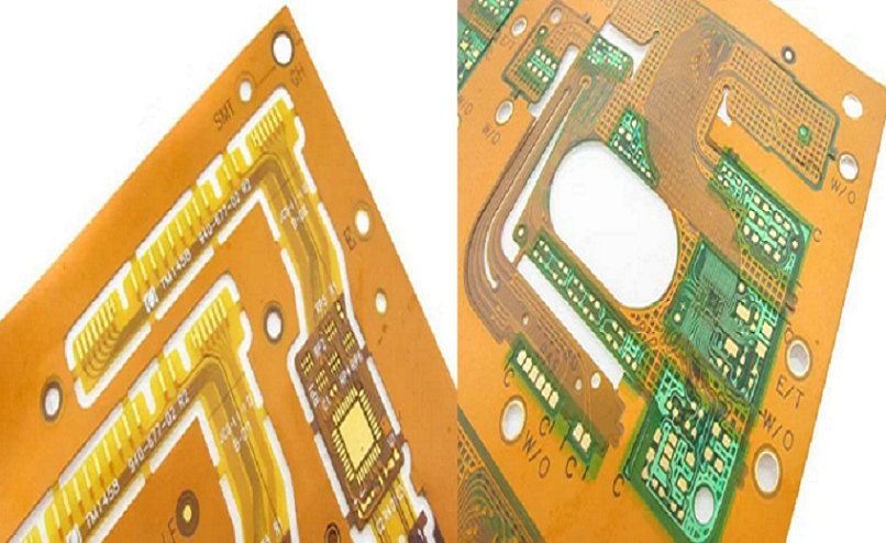
What is Flexible PCB Coverlay
Structure & Material Composition
- Base film: 12.5μm, 25μm, or 50μm polyimide (PI) per IPC-4203
- Adhesive layer: 12–25μm modified acrylic or epoxy adhesive
- Total thickness: 25–75μm standard (PI + adhesive)
- Temperature resistance: -55°C to +150°C continuous, 260°C peak for 10s
- Dielectric strength: >30kV/mm, volume resistivity >10¹⁶Ω·cm
Application Process & Performance
- Laser-cut or die-cut to match circuit patterns before lamination
- Laminated at 160–180°C, 10–15kg/cm² pressure for 60–90 minutes
- Registration accuracy: ±20μm layer-to-layer alignment
- Minimum feature: 0.2mm coverlay web width between openings
- Bend performance: >10,000 dynamic flex cycles without cracking
What is Flexible Solder Mask
Material & Processing Characteristics
- Liquid photoimageable (LPI) epoxy-based ink formulation
- Applied via screen printing or curtain coating at 10–18μm thickness
- UV-exposed and developed to create precise protective patterns
- Thermal cure: 120–150°C for 30–60 minutes
- Minimum feature: 50μm solder dam between 0.3mm pitch pads
Physical & Electrical Properties
- Dielectric constant: 3.5–4.5 at 1MHz
- Volume resistivity: >10¹⁵Ω·cm after curing
- Flex life: Limited to <1,000 dynamic bending cycles
- Color options: green, black, white, yellow, blue
- Adhesion strength: ≥4B per ASTM D3359 cross-hatch test
Learn more about : What Is Flexible PCB
Key Comparison Table: Coverlay vs Solder Mask
| Parameter | Polyimide Coverlay | Flexible LPI Solder Mask | Critical Difference |
|---|---|---|---|
| Base Material | Polyimide film + adhesive | Epoxy-based liquid ink | Mechanical flexibility |
| Total Thickness | 25–75μm | 10–18μm | Profile height |
| Minimum Feature | 0.2mm web width | 50μm solder dam | Resolution capability |
| Dynamic Flex Life | >10,000 cycles | <1,000 cycles | Bending endurance |
| Temperature Resistance | -55°C to +150°C | -40°C to +125°C | Thermal stability |
| Application Method | Lamination | Printing/coating + UV cure | Process complexity |
| Cost | +30–40% | Standard | Economic factor |
| Moisture Barrier | Excellent (MVTR <5g/m²/day) | Good (MVTR 10–15g/m²/day) | Environmental protection |
| Chemical Resistance | Superior to acids/solvents | Good to most chemicals | Chemical durability |
Key Aspects of Coverlay in Flex PCBs
Primary Benefits
- Exceptional mechanical flexibility for repeated bending
- Superior moisture and chemical resistance
- Excellent thermal stability for high-temperature assembly
- Robust dielectric insulation for high-voltage applications
- Long-term reliability in harsh environments
Limitations & Design Constraints
- Larger minimum feature size (0.2mm vs 50μm for solder mask)
- Higher material and processing costs
- Registration challenges with fine-pitch circuits
- Limited availability in thickness <25μm
- Adhesive squeeze-out risk during lamination (controlled to <10μm)
Key Aspects of Flexible Solder Mask
Advantages for Flexible Circuits
- Ultra-fine feature resolution for high-density designs
- Lower overall profile (10–18μm vs 25–75μm)
- Cost-effective for large-scale production
- Complete coverage with no gaps or overlaps
- Compatibility with automated optical inspection (AOI)
Disadvantages & Application Limits
- Poor performance under repeated dynamic bending
- Lower thermal resistance compared to polyimide
- Potential cracking during extreme temperature cycling
- Reduced chemical resistance to harsh solvents
- Limited effectiveness for thickness <0.1mm flexible substrates
Learn more about: What Is a Flexible Printed Circuit?
Key Design Considerations
Thickness & Material Selection
- Coverlay: Match thickness to flex requirements (25μm for dynamic, 50μm for static)
- Solder mask: Maintain 10–15μm uniform thickness across entire panel
- Rigid-flex transition: Use coverlay for flex zones, solder mask for rigid sections
- Adhesive selection: Low-flow acrylic for coverlay (≤10μm squeeze-out), epoxy for solder mask
Registration & Feature Design
- Coverlay openings: 0.1mm larger than solder pads perimeter
- Solder mask expansion: 50–75μm beyond pad edges (IPC-2221)
- Minimum web width: 0.2mm for coverlay, 50μm for solder mask
- Bend radius: Coverlay supports ≥6× thickness, solder mask ≥15× thickness
Application Scenarios & Best Uses
Ideal Coverlay Applications
- Dynamic flex applications (wearables, hinges, cameras)
- High-temperature environments (automotive, industrial)
- Long-term reliability requirements (medical, aerospace)
- High-moisture or chemical exposure conditions
- Rigid-flex PCB flexible sections
Optimal Solder Mask Applications
- High-density flexible circuits with fine-pitch components
- Static flex or minimal bending applications
- Cost-sensitive consumer electronics
- Single-sided or double-sided flexible PCB prototypes
- Rigid sections of rigid-flex assemblies
Manufacturing Verification & Quality Control
Coverlay Quality Checks
- Post-lamination void inspection: <1% void area allowed
- Adhesive squeeze-out control: <10μm beyond edges
- Peel strength test: ≥1.0N/mm per IPC-6012 Class 3
- Thermal cycling: -40°C to +125°C, 100 cycles with no delamination
- Flex testing: 1,000 cycles without cracking or lifting
Solder Mask Quality Assurance
- Film thickness uniformity: ±2μm across panel
- Adhesion testing: ASTM D3359 4B minimum
- Solder resistance: 260°C, 3× reflow with no blistering
- Resolution verification: 50μm minimum features fully defined
- Electrical isolation: ≥100MΩ between adjacent conductors
Core Technical Parameters
- Coverlay thickness: 25μm (12.5μm PI + 12.5μm adhesive), 50μm (25μm PI + 25μm adhesive)
- Solder mask thickness: 10–18μm (liquid photoimageable)
- Minimum line/space: 40μm/40μm with solder mask, 50μm/50μm with coverlay
- Registration accuracy: ±20μm (coverlay), ±15μm (solder mask)
- Bend radius: Static ≥6× thickness (coverlay), ≥15× thickness (solder mask)
- Temperature range: -55°C to +150°C (coverlay), -40°C to +125°C (solder mask)
- IPC standards: IPC-4203 (flex materials), IPC-6012 (qualification), IPC-2221 (design)
Case Study
Project Overview
6-layer rigid flex PCB for medical implant: 4 rigid layers, 2 flex layers, 0.6mm total thickness, 0.3mm pitch BGA (160 pins), 50μm line/space, operating temperature -40°C to +85°C, 5,000+ flex cycles requirement.
Initial Approach & Challenges
- Initially specified LPI solder mask for entire assembly
- Flex zones failed after 800 bending cycles (cracking at solder mask)
- Insufficient insulation resistance in humid environment (85% RH)
- First-pass yield: 72% due to registration issues with fine features
- Field failures reported after 3 months of operation
Process Optimization
- Converted flex regions to 25μm polyimide coverlay (12.5μm PI + 12.5μm adhesive)
- Retained solder mask on rigid sections for fine-pitch BGA
- Optimized coverlay lamination: 170°C, 12kg/cm², 75 minutes
- Implemented strict adhesive squeeze-out control (<10μm)
- Added post-lamination baking (120°C, 60 minutes) for stress relief
Final Results
- Flex life extended to 12,000+ cycles without failure
- Insulation resistance maintained >100MΩ after 1,000 hours humidity testing
- First-pass yield improved to 91%
- Zero field failures during 12-month validation
- Overall assembly thickness reduced by 30μm in flex zones
Common Design Errors
Coverlay Design Mistakes
- Specifying <0.2mm coverlay web width between openings
- Designing coverlay openings same size as pads (requires +0.1mm perimeter)
- Placing coverlay seams across dynamic bend lines
- Using excessive adhesive thickness (>25μm) causing squeeze-out
- Ignoring registration tolerance (+20μm) in fine-pitch designs
Solder Mask Design Errors
- Applying solder mask to dynamic flex zones (>1,000 cycles)
- Designing <50μm solder dams between fine-pitch pads
- Inconsistent thickness across panel (variation >±2μm)
- Insufficient cure time/temperature leading to poor adhesion
- Missing solder mask expansion (requires 50–75μm beyond pads)
Combined Material Misapplications
- Using coverlay on high-density rigid sections with <0.2mm features
- Applying solder mask to high-temperature applications (>125°C)
- Mixing materials without proper transition design
- Ignoring bend radius requirements for selected protection type
- Inadequate testing validation for specific application conditions
Frequently Asked Questions
Q1: When should I choose coverlay instead of solder mask for flexible PCB?
A1: Select polyimide coverlay for applications requiring >1,000 dynamic flex cycles, operating temperatures >125°C, superior moisture protection, or long-term reliability in harsh environments.
Q2: Can I use both coverlay and solder mask on the same flexible printed circuit?
A2: Yes—this is common in rigid-flex PCB designs. Use coverlay on dynamic flex zones and solder mask on rigid sections with fine-pitch components for optimal performance and cost balance.
Q3: What thickness of coverlay is recommended for dynamic bending applications?
A3: For dynamic flex applications, 25μm total coverlay thickness (12.5μm polyimide + 12.5μm adhesive) provides best flexibility while maintaining protection. Static applications can use 50μm thickness.
Q4: What IPC standards govern coverlay and solder mask specifications?
A4: Flexible PCB protection materials follow IPC-4203 (flex materials), IPC-6012 (qualification and performance), and IPC-2221 (generic design standards) for consistent manufacturing and performance.
If you need professional flexible circuit board design support or quotation, our team provides free DFM check and fast turnaround.


![Understanding PCB Costs & Pricing [Your Complete Guide]](https://hdicircuitboard.com/wp-content/uploads/elementor/thumbs/Understanding-PCB-Costs-Pricing-Your-Complete-Guide-qzzhe6mcaxuolkux3xalfktgavumi9y1aqfbs9bpv4.webp "Understanding PCB Costs & Pricing [Your Complete Guide]")


