
Selecting between adhesive-based and adhesiveless flexible PCB constructions, along with choosing rolled annealed (RA) or electrodeposited (ED) copper foil, directly defines bend performance, thermal stability, signal integrity, and manufacturing cost in flexible printed circuit and rigid flex PCB designs. Adhesive-based structures offer lower cost and simpler processing, while adhesiveless designs deliver thinner dielectrics, higher frequency performance, and improved flex endurance. RA copper provides exceptional ductility for dynamic bending, and ED copper delivers consistent thickness and lower cost for static or low‑cycle applications. All selections must align with IPC‑4203 material standards and IPC‑2223 design rules to ensure reliability in bendable circuit board applications.
Learn more about: What is a Flexible Circuit Board? A Complete Guide for Beginners
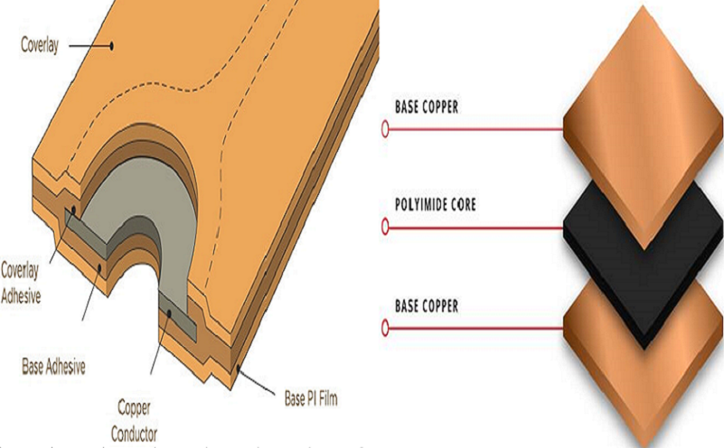
Adhesive‑Based Flexible PCB Construction
Layer Structure & Material Parameters
Adhesive‑based flexible circuits use a bonding layer to join copper foil to polyimide dielectric films.
- Typical layer composition: Cu foil → acrylic or epoxy adhesive (12.5–25μm) → polyimide base film (25–50μm)
- Total dielectric thickness: 37.5–75μm including adhesive layer
- Adhesive type: modified acrylic (standard) or high‑temperature epoxy
- Glass transition temperature (Tg): 80–120°C for acrylic adhesives
- Peel strength: 0.8–1.0 N/mm per IPC‑6012 Class 2 requirements
- Moisture absorption: 1.5–2.5% under 85°C/85%RH conditions
Advantages & Application Suitability
- Lower material cost compared to adhesiveless constructions
- Compatible with standard lamination equipment and production lines
- Suitable for low‑to‑medium dynamic bend cycles (<5,000 cycles)
- Effective for single‑sided and double‑sided flexible pcb board designs
- Widely used in consumer electronics and static interconnect applications
- Supports standard coverlay lamination and rigid‑flex integration
Limitations & Manufacturing Risks
- Adhesive squeeze‑out during lamination (up to 15μm without process control)
- Higher dielectric loss due to adhesive material properties
- Reduced thermal stability limiting high‑temperature assembly
- Increased risk of delamination during thermal cycling
- Thicker overall construction limiting minimum bend radius
- Higher moisture absorption impacting long‑term insulation resistance
Adhesiveless Flexible PCB Construction
Structural Design & Physical Properties
Adhesiveless flexible circuits bond copper foil directly to polyimide through high‑pressure casting or lamination without intermediate adhesive layers.
- Layer structure: copper foil directly cast onto polyimide film
- Total dielectric thickness: 25–50μm (polyimide only)
- Dielectric constant (Dk): 3.4–3.6 stable across frequency ranges
- Dissipation factor (Df): <0.008 at 1GHz for high‑frequency performance
- Temperature resistance: continuous operation up to 150°C
- Peel strength: 1.0–1.4 N/mm, exceeding IPC‑6012 Class 3 requirements
Performance Benefits & Ideal Uses
- Ultra‑thin profile enabling smaller bend radii
- Superior thermal stability for lead‑free reflow assembly
- Improved signal integrity for high‑speed digital and RF designs
- Extended flex life exceeding 100,000 dynamic bending cycles
- Lower moisture absorption (<0.8%) for harsh environment applications
- Preferred for medical, automotive, and aerospace rigid flex PCB designs
Cost & Production Considerations
- Higher raw material cost compared to adhesive‑based constructions
- Requires specialized casting and lamination equipment
- Tighter process control during manufacturing
- Longer lead times for specialized material procurement
- Improved yield in high‑reliability and high‑cycle applications
- Reduced assembly failures in dynamic flex environments
Learn more about: What is a Flexible PCB? A Complete Guide for Beginners
Adhesive vs Adhesiveless Flex PCB Comparison Table
| Parameter | Adhesive‑Based Flex | Adhesiveless Flex | Performance Difference |
|---|---|---|---|
| Total Dielectric Thickness | 37.5–75μm | 25–50μm | 33% thinner profile |
| Dynamic Flex Cycles | <5,000 cycles | >100,000 cycles | 20x longer endurance |
| Temperature Resistance | 80–120°C | –55°C to +150°C | 30°C higher stability |
| Moisture Absorption | 1.5–2.5% | <0.8% | 60% lower absorption |
| Dissipation Factor (Df) | 0.015–0.025 | <0.008 | 50% better signal integrity |
| Peel Strength (N/mm) | 0.8–1.0 | 1.0–1.4 | 40% higher adhesion |
| Relative Cost | 1.0x (base) | 1.4–1.8x | 40–80% premium |
| Minimum Bend Radius | 8× thickness | 4× thickness | 50% tighter bending |
RA vs ED Copper Foil for Flexible PCBs
Material Formation & Structural Differences
Copper foil type dominates flex life, surface quality, and manufacturability in flexible printed circuit designs.
Rolled Annealed (RA) Copper
- Formed by compressing and annealing cast copper ingots
- Grain structure: uniform, elongated, highly ductile lattice
- Surface roughness (Rz): 0.8–1.5μm
- Standard thickness: 5μm, 9μm, 12μm, 18μm
- IPC classification: IPC‑4562 Type RA foil
Electrodeposited (ED) Copper
- Deposited electrolytically onto rotating drums
- Grain structure: columnar, directional, lower ductility
- Surface roughness (Rz): 2.0–3.5μm
- Standard thickness: 12μm, 18μm, 35μm
- IPC classification: IPC‑4562 Type ED foil
Flexibility & Fatigue Resistance
RA copper provides significantly improved performance in dynamic bending environments.
- RA copper flex life: 10,000–100,000+ bending cycles
- ED copper flex life: 1,000–5,000 bending cycles
- RA elongation: 10–15% under tensile stress
- ED elongation: 2–5% under identical loading
- RA preferred for dynamic flex, hinges, wearables, and repeated motion
- ED suitable for static flex, rigid‑flex rigid regions, and low‑cycle applications
Cost, Surface Quality & Manufacturing Impact
- ED copper: lower cost, consistent thickness, wide availability
- RA copper: 15–30% cost premium, improved ductility
- ED surface: rougher, improves solder mask and adhesive bonding
- RA surface: smoother, improves impedance control in high‑speed designs
- ED better for fine line etching down to 30μm/30μm
- RA reduces copper cracking during dynamic flexing
- ED foil standard for low‑cost consumer bendable circuit board products
RA vs ED Copper Performance Comparison Table
| Characteristic | RA Copper Foil | ED Copper Foil | Practical Impact |
|---|---|---|---|
| Flex Cycle Life | 10,000–100,000+ | 1,000–5,000 | RA = 20x longer life |
| Elongation Percentage | 10–15% | 2–5% | RA more ductile |
| Surface Roughness (Rz) | 0.8–1.5μm | 2.0–3.5μm | ED better for bonding |
| Relative Cost | 1.15–1.30x | 1.0x (base) | ED lower cost |
| Minimum Line/Space | 40μm/40μm | 30μm/30μm | ED supports finer features |
| Thermal Stability | Excellent | Good | Similar high‑temp performance |
| Impedance Control | ±4% | ±6% | RA more consistent |
Material Selection Guidelines
Choosing Adhesive or Adhesiveless Construction
Select adhesive‑based flex PCB under these conditions:
- Cost‑sensitive consumer electronics applications
- Static or low‑cycle bending requirements (<5,000 cycles)
- Standard production timelines and budgets
- Low‑frequency signal designs without strict loss constraints
- Double‑sided flexible circuits with conventional assembly
Select adhesiveless flex PCB for these use cases:
- High‑cycle dynamic bending applications (>10,000 cycles)
- High‑speed RF, microwave, and GHz‑range digital designs
- Medical, automotive, and aerospace rigid flex PCB systems
- Ultra‑thin form factor and tight bend radius requirements
- High‑temperature lead‑free assembly environments
Learn more about: Flexible PCB: A Comprehensive Guide to Features, Applications, Types & Key Considerations
Choosing RA or ED Copper Foil
Select RA copper foil when:
- Dynamic flexing, repeated bending, or hinge applications
- Medical wearables, portable devices, and camera modules
- Long‑term reliability under thermal and mechanical stress
- Flex life exceeding 10,000 cycles is required
- Minimizing copper cracking and fatigue is critical
Select ED copper foil when:
- Static flex or minimal bending environments
- Cost‑optimized high‑volume production
- Fine‑pitch, fine‑line high‑density interconnect designs
- Rigid sections of rigid‑flex assemblies
- Standard consumer electronics with low reliability requirements
Quality Control & IPC Compliance Standards
Material Qualification & Testing
All flexible PCB materials must comply with strict industry standards.
- IPC‑4203: specification for flexible dielectric materials
- IPC‑4562: copper foil performance and classification standards
- IPC‑6012: qualification and performance specifications
- Peel strength testing per IPC‑TM‑650 2.4.9 method
- Thermal cycling: –40°C to +125°C for 100 cycles minimum
- Flex endurance testing per IPC‑2223 dynamic bend requirements
Manufacturing Process Controls
- Adhesive squeeze‑out limited to <10μm during lamination
- Layer registration tolerance maintained at ±20μm
- Copper thickness uniformity controlled within ±1μm
- Vacuum lamination at 170–180°C with 15–20 kg/cm² pressure
- 100% visual inspection for delamination and voiding
- Electrical testing verifying insulation resistance >100MΩ
Learn more about: What Is Flexible PCB
Core Technical Parameters
- Adhesive thickness: 12.5–25μm (acrylic/epoxy)
- Adhesiveless polyimide thickness: 25–50μm
- RA copper thickness: 5μm, 9μm, 12μm, 18μm
- ED copper thickness: 12μm, 18μm, 35μm
- Minimum line/space: 30μm/30μm (ED), 40μm/40μm (RA)
- Minimum bend radius: 4× thickness (adhesiveless), 8× thickness (adhesive)
- Dielectric constant (Dk): 3.4–3.6 (adhesiveless), 3.6–4.0 (adhesive)
- Operating temperature: –55°C to +150°C (adhesiveless), –40°C to +120°C (adhesive)
- IPC standards: IPC‑2223, IPC‑4203, IPC‑4562, IPC‑6012
Case Study
Project Overview
4‑layer rigid flex PCB for portable medical monitoring device: 2 flex layers, 2 rigid layers, adhesiveless polyimide dielectric, 0.1mm flex thickness, 40μm/40μm line/space, 10,000+ dynamic bend cycle requirement, operating temperature –40°C to +85°C.
Initial Challenges
- Original design used adhesive‑based construction with ED copper
- Flex failures occurred at 2,800 cycles (copper cracking & adhesive delamination)
- Moisture absorption caused insulation resistance drops below 100MΩ
- Signal degradation observed in high‑frequency sensor circuits
- First‑pass manufacturing yield: 71%
Process & Material Improvements
- Converted from adhesive‑based to adhesiveless polyimide structure
- Replaced 18μm ED copper with 12μm rolled annealed (RA) foil
- Optimized lamination cycle: 175°C, 18 kg/cm², 70 minutes
- Implemented strict adhesive‑free layer bonding controls
- Added post‑lamination stress relief baking at 120°C for 60 minutes
Final Results
- Flex life extended to 12,000+ cycles without failures
- Insulation resistance stabilized above 100MΩ in humid environments
- High‑frequency signal integrity improved by 35%
- First‑pass yield increased to 90.4%
- Zero field failures recorded during 12‑month customer validation
- Overall assembly thickness reduced by 22% in flex regions
Common Design Errors
Material Selection Mistakes
- Specifying adhesive‑based construction for >5,000 flex cycles
- Using ED copper in high‑dynamic wearable or hinge applications
- Selecting adhesiveless materials for cost‑only consumer designs
- Mismatching dielectric CTE with copper foil causing delamination
- Ignoring IPC‑4203 thickness and performance specifications
Stackup & Processing Errors
- Inadequate control of adhesive squeeze‑out (>15μm)
- Designing below minimum bend radius for selected material
- Placing components within 1mm of dynamic flex zones
- Asymmetric layer construction causing warpage >0.5%
- Insufficient peel strength design leading to premature delamination
Copper & Trace Layout Errors
- Using >18μm copper thickness in dynamic flex regions
- Routing traces parallel to bend axis creating stress points
- Trace width <0.2mm in high‑cycle flex areas
- Missing teardrop connections at via transitions
- Inconsistent copper distribution creating mechanical imbalance
Frequently Asked Questions
Q1: When should I use adhesiveless flexible PCB construction?
A1: Adhesiveless construction is recommended for designs requiring more than 5,000 dynamic flex cycles, high‑frequency signal integrity, ultra‑thin profiles, or high‑temperature operational stability.
Q2: Is RA copper always better for flexible printed circuit designs?
A2: RA copper provides superior flex life but costs 15–30% more. ED copper is preferred for static flex, fine‑line layouts, and cost‑sensitive applications with low bending requirements.
Q3: What is the minimum bend radius difference between adhesive and adhesiveless materials?
A3: Adhesiveless materials support a 4× thickness bend radius, while adhesive‑based constructions require 8× thickness, allowing adhesiveless designs to achieve 50% tighter bending.
Q4: Which IPC standards govern flexible PCB material selection?
A4: Key standards include IPC‑4203 for flexible dielectrics, IPC‑4562 for copper foils, IPC‑2223 for flex design rules, and IPC‑6012 for performance and qualification requirements.
If you need professional flexible circuit board design support or quotation, our team provides free DFM check and fast turnaround.
Learn more about: What Is a Flexible Printed Circuit?


![Understanding PCB Costs & Pricing [Your Complete Guide]](https://hdicircuitboard.com/wp-content/uploads/elementor/thumbs/Understanding-PCB-Costs-Pricing-Your-Complete-Guide-qzzhe6mcaxuolkux3xalfktgavumi9y1aqfbs9bpv4.webp "Understanding PCB Costs & Pricing [Your Complete Guide]")


