
Blind and buried vias form the core structural elements of high-density interconnect (HDI) PCB systems, enabling targeted layer-to-layer electrical connections without full-board drilling. Blind vias connect outer layers to internal layers, while buried vias link only internal layers, both supporting miniaturization, high-speed signal integrity, and dense routing in modern electronics. All design and fabrication parameters follow IPC‑2221, IPC‑2226, and IPC‑6012 specifications, with strict control over drill size, aspect ratio, plating thickness, and layer registration for consistent performance in mass production.
Learn more about: What are Blind Vias & Buried Vias in HDI?
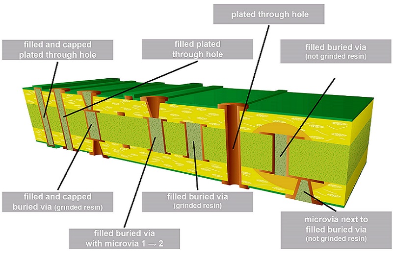
What Are Blind & Buried Vias in HDI PCBs
Blind Vias
Blind vias extend from an external layer to one or more internal layers without penetrating the full thickness of the circuit board.
- Typical connections: L1→L2, L1→L3, L8→L7, or L8→L6 in multi-layer structures
- Drill diameter range: 75μm to 150μm for standard HDI production
- Aspect ratio (depth to diameter): controlled at 0.75:1 or lower
- Minimum annular ring: 50μm as defined in IPC‑2221 generic design rules
- Primary drilling method: UV laser for precision depth control
Buried Vias
Buried vias exist entirely between internal layers and are fully enclosed after lamination, with no exposure on either board surface.
- Typical connections: L2→L3, L3→L4, L4→L6 in multi-layer core structures
- Drill diameter range: 100μm to 200μm for stable plating performance
- Aspect ratio limited to 1:1 for consistent copper coverage
- Fabricated during sub-core assembly before full stack lamination
- Primarily formed using mechanical drilling for inner-layer sub-cores
Learn more about: HDI PCB Design Guidelines
Sequential Lamination and Manufacturing Flow
Sub-Core Fabrication for Buried Vias
Buried vias require staged sub-core production to maintain structural and electrical integrity.
- Fabricate inner layer sub-cores with patterned copper circuitry
- Mechanically drill buried vias at targeted locations
- Perform desmear and electroless copper deposition
- Plate vias to 18μm–25μm copper thickness per IPC‑6012
- Laminate sub-cores under controlled temperature and pressure
Laser Drilling and Build-Up for Blind Vias
Blind vias rely on post-core laser drilling to achieve precise depth and location accuracy.
- Laser drilling achieves depth tolerance within ±10μm
- Plasma desmear removes resin residue for reliable plating adhesion
- Direct copper plating ensures uniform wall coverage
- Build-up dielectric layers range from 40μm to 75μm in thickness
- Final layer registration controlled to ±20μm across the panel
Learn more about: Microvia HDI PCB: What You Need to Know
Key Advantages of Blind & Buried Vias
Higher Routing Density and Layout Efficiency
- Eliminate the need for full through-vias that occupy surface routing area
- Enable up to 50% greater routing density in fine-pitch BGA regions
- Support two to three escape rows under 0.5mm–0.65mm pitch BGAs
- Reduce total layer count by one to two layers in complex systems
- Allow tighter component placement without routing conflicts
Superior Electrical and Signal Integrity Performance
- Shorten signal transmission paths and reduce parasitic inductance by 40%–60%
- Limit via stub length to below 20μm for high-speed serial links
- Maintain impedance control at ±5% for 50Ω single-ended and 100Ω differential lines
- Reduce EMI radiation by confining return currents within internal planes
- Improve eye diagram performance for 28Gbps, 56Gbps, and 112Gbps PAM4 signals
Enhanced Thermal Management Capability
- Create direct thermal paths from high-power ICs to internal ground planes
- Lower thermal resistance by 25%–35% compared to through-via structures
- Support dense thermal via arrays in compact component footprints
- Improve heat dissipation in wearable, mobile, and automotive designs
- Reduce hot-spot temperature by 10°C–15°C under high-load conditions
Critical Design and Manufacturing Considerations
Aspect Ratio and Geometric Constraints
- Blind vias: maximum aspect ratio fixed at 0.75:1 for production stability
- Buried vias: maximum aspect ratio limited to 1:1 to avoid plating gaps
- Minimum drill-to-copper clearance: 75μm on all internal layers
- Minimum via-to-via spacing: 150μm to prevent electrical shorting
- Trace and space capability down to 50μm/50μm for HDI microvias pcb structures
Stackup Symmetry and Via Placement
- Symmetric layer stackups reduce warpage to below 0.2% per IPC standards
- Overlapping blind and buried vias must be strictly avoided
- Staggered via patterns improve structural rigidity and lamination quality
- 1+N+1 and 2+N+2 stackup formats deliver optimal reliability
- Layer-to-layer registration controlled within ±20μm for fine-feature designs
Material Selection for HDI Performance
- High-Tg laminate systems with Tg ≥170°C for reflow stability
- Low CTE substrates with α1 ≤50 ppm/°C to reduce thermal stress
- Dielectric materials compatible with laser drilling and desmear processes
- Bonding film thickness from 25μm to 50μm for sub-lamination stages
- Materials compliant with IPC‑4101 for rigid HDI PCB fabrication
Comparative Tables
Blind Via vs. Buried Via vs. Microvia Comparison
| Parameter | Blind Via | Buried Via | Microvia |
|---|---|---|---|
| Connection Range | Outer to Inner Layers | Inner to Inner Layers | Adjacent HDI Layers |
| Drill Technology | Laser or Mechanical | Mechanical | Laser Only |
| Standard Diameter | 75–200μm | 100–200μm | 50–125μm |
| Aspect Ratio Limit | ≤0.75:1 | ≤1:1 | ≤0.75:1 |
| Surface Visibility | Visible | Not Visible | Visible or Internal |
| Relative Cost | Medium | High | Very High |
Blind/Buried Vias vs. Through-Hole Vias Comparison
| Performance Feature | Blind & Buried Vias | Through-Hole Vias |
|---|---|---|
| Routing Efficiency | Excellent | Limited |
| Surface Layout Usage | Efficient | High Consumption |
| Signal Integrity | Excellent | Reduced by Long Stubs |
| Parasitic Inductance | Low | High |
| Production Cost | 20–40% Higher | Standard |
| Layer Count Efficiency | Reduces Total Layers | Requires Extra Layers |
Technical Specifications
- Minimum blind via diameter: 75μm
- Minimum buried via diameter: 100μm
- Copper plating thickness: 18–25μm
- Annular ring requirement: 50μm minimum
- Internal clearance: 75μm minimum
- Aspect ratio: blind vias ≤0.75:1, buried vias ≤1:1
- Trace/space resolution: 50μm/50μm
- Impedance tolerance: ±5%
- Layer registration: ±20μm
- Allowable via voiding: <1%
Case Study
Project Overview
Board type: 10‑layer 2+6+2 HDI PCB; application: 5G optical communication module; BGA pitch: 0.5mm; stack includes L1→L2 blind vias, L3→L4 buried vias, and L2→L7 internal connections.
Issues Encountered
- Blind via aspect ratio reached 1:1, exceeding the 0.75:1 production limit
- Via overlap caused internal layer shorting during electrical test
- Annular ring width reduced to 35μm, below the required 50μm minimum
- Plating void rate reached 3.1%, far exceeding the <1% IPC limit
- Impedance deviation measured at ±8%, outside the ±5% tolerance window
Corrective Actions Implemented
- Redesigned blind vias to 125μm diameter with 90μm depth for 0.72:1 ratio
- Increased annular ring to 60μm and clearance to 80μm
- Reconfigured via placement to eliminate overlapping structures
- Optimized plating parameters and implemented vacuum filling
- Adjusted trace geometries to stabilize impedance within ±4.2%
Final Results
- Overall production yield improved from 67% to 94.7%
- Plating voids reduced to 0.6%, meeting IPC‑6016 requirements
- Impedance consistency maintained across all high-speed channels
- No delamination or cracking observed after 1000 thermal cycles
- Full compliance with IPC‑6012 Class 3 and hdi pcb manufacturing standards
Common Design Errors
- Aspect ratios exceeding 0.75:1 for blind vias lead to incomplete plating and open circuits.
- Insufficient annular rings below 50μm cause fracture failures during thermal cycling.
- Overlapping blind and buried vias create delamination risks and electrical shortages.
- Asymmetric stackups induce excessive warpage and registration misalignment.
- Inadequate drill-to-copper clearance results in etching shorts and low production yield.
- Standard low-Tg materials fail reflow compatibility and long-term reliability tests.
Quality Control and Reliability Testing
Factory Testing Protocols
- Microsection analysis to verify plating uniformity and annular ring dimensions
- Coordinate measuring machine validation of drill size and location accuracy
- 100% electrical open/short testing per IPC‑TM‑650
- Thermal shock testing from ‑40°C to 125°C over 100 to 500 cycles
- Triple reflow simulation at 260°C for assembly compatibility
- TDR impedance measurement for controlled high-speed transmission lines
Industry Compliance Standards
- IPC‑2221: Generic printed board design standard
- IPC‑2226: Sectional design standard for HDI microvias pcb
- IPC‑6012: Qualification and performance specification for rigid PCBs
- IPC‑6016: Reliability standard for microvia and HDI structures
- IPC‑4101: Laminate material specification for rigid printed boards
- UL 94V‑0, RoHS, IATF 16949, and ISO 9001 certifications
Applications of Blind & Buried Vias
High-Density Consumer Electronics
- Smartphones, tablets, and wearable electronic devices
- Compact camera modules and sensor assemblies
- High-speed memory modules and solid-state storage devices
- Miniaturized medical monitoring and diagnostic equipment
Industrial and High-Speed Systems
- 5G and 6G wireless communication infrastructure
- Automotive ADAS controllers and infotainment systems
- Industrial IoT gateways and edge computing processors
- RF, microwave, and high-frequency analog assemblies
When to Implement Blind & Buried Vias
Recommended Application Scenarios
- BGA pitch at 0.65mm or below requiring dense fanout routing
- High-speed signals above 5Gbps demanding low-stub interconnects
- Designs targeting layer count reduction for cost and weight optimization
- High-power components requiring focused thermal dissipation paths
- Space-constrained form factors in mobile and portable electronics
Less Suitable Applications
- BGAs with pitch of 1.0mm or larger with standard fanout capability
- Low-speed, low-density circuits with no miniaturization requirements
- Extreme cost-sensitive projects with minimal layer complexity
- Low-volume prototype builds below 50 units
Frequently Asked Questions
Q1: What is the maximum allowable aspect ratio for blind vias in HDI PCBs?
A1: The industry standard defined in IPC‑2226 sets a maximum aspect ratio of 0.75:1 for reliable plating and long-term performance.
Q2: Are overlapping blind and buried vias acceptable in HDI design?
A2: Overlapping vias create structural weakness and delamination risks; a minimum spacing of 150μm must be maintained between structures.
Q3: How much additional cost do blind and buried vias add to production?
A3: Blind vias typically increase cost by 20–30%, while buried vias add 30–45% due to sequential lamination and laser processing.
Q4: Which stackup structure is most reliable for blind and buried via designs?
A4: Symmetric 2+N+2 HDI stackups provide the best stability, registration control, and impedance consistency for high-volume production.
If you need professional HDI PCB design support or quotation, our team provides free DFM check and fast turnaround.


![Understanding PCB Costs & Pricing [Your Complete Guide]](https://hdicircuitboard.com/wp-content/uploads/elementor/thumbs/Understanding-PCB-Costs-Pricing-Your-Complete-Guide-qzzhe6mcaxuolkux3xalfktgavumi9y1aqfbs9bpv4.webp "Understanding PCB Costs & Pricing [Your Complete Guide]")


