PCB Assembly Services for Engineers
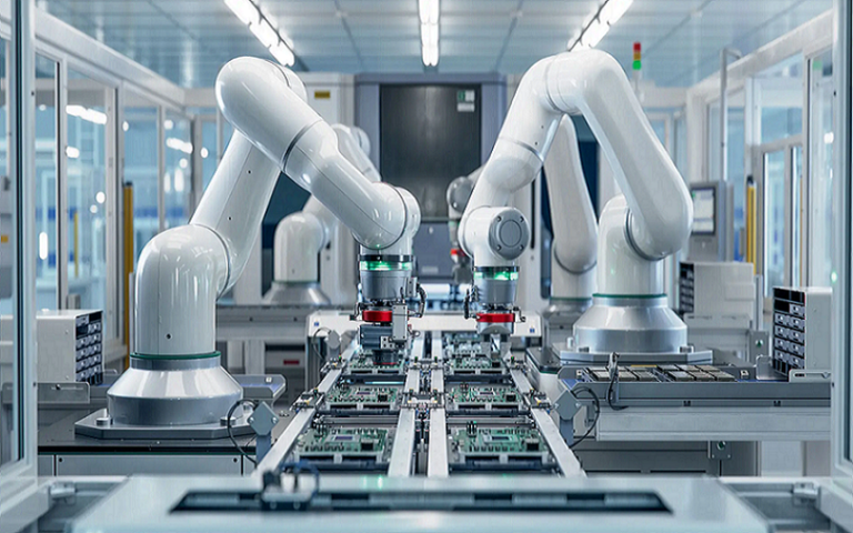
PCB assembly services convert a bare printed circuit board into a tested PCBA by combining solder paste printing, component placement,…
PCB assembly services convert a bare printed circuit board into a tested PCBA by combining solder paste printing, component placement,…
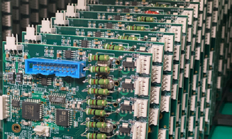
PCB assembly is the manufacturing process that turns a bare printed circuit board into a functional electronic assembly by applying…
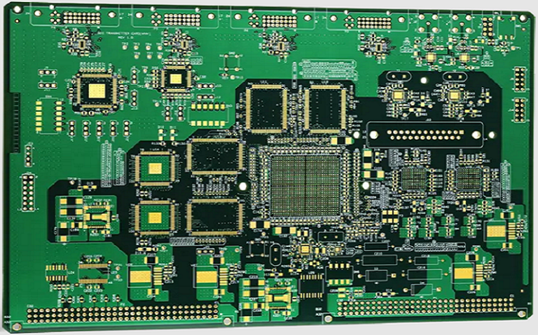
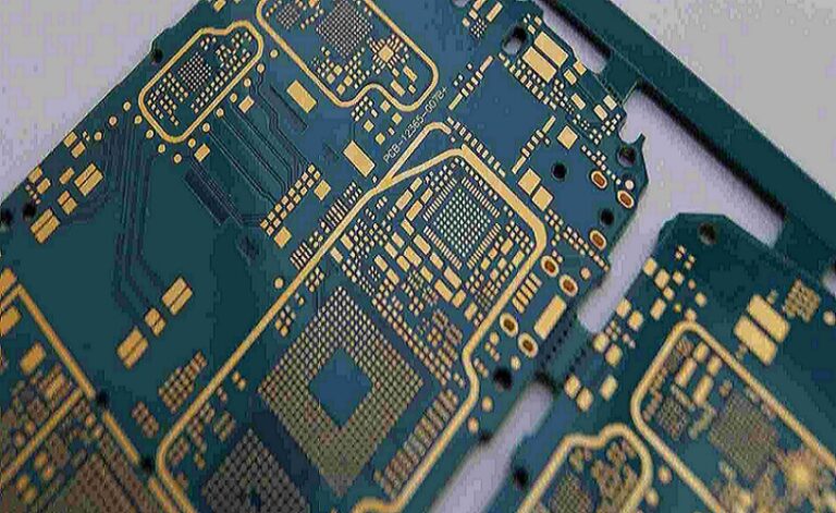
HDI PCB fabrication capabilities define what a factory can repeatedly manufacture across trace width, spacing, laser microvias, via-in-pad, sequential build-up,…
HDI PCB prototype services turn dense PCB designs into testable boards by validating microvias, via-in-pad, sequential lamination, fine-pitch routing, stackup…
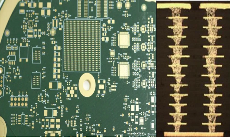
HDI PCB for fine-pitch BGA is required when BGA ball pitch, package size, escape routing density, and assembly yield exceed…
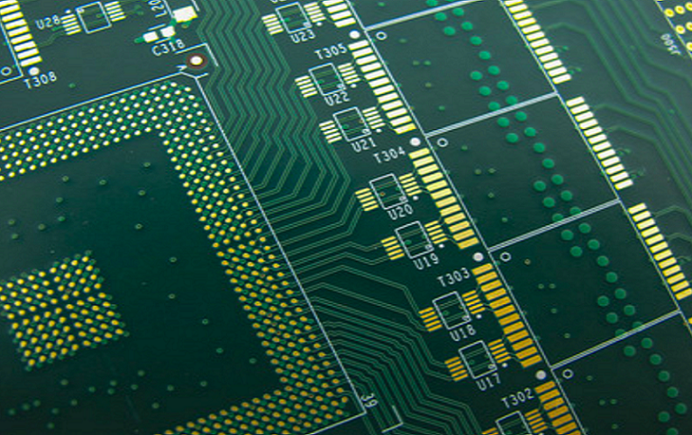
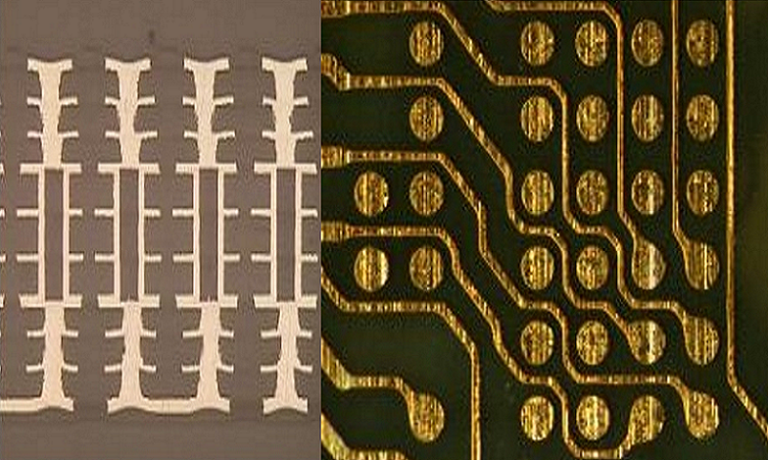
HDI PCB stackup design defines how signal layers, power planes, ground planes, buildup dielectrics, microvias, buried vias, via-in-pad structures, and…
HDI PCB design should start with stack-up planning, microvia selection, fine-pitch BGA breakout, material choice, controlled impedance, and DFM review…
HDI PCB for TPU hardware uses high density interconnect structures, high-layer count stackups, low Dk materials, microvias, via-in-pad, sequential lamination,…
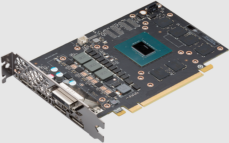
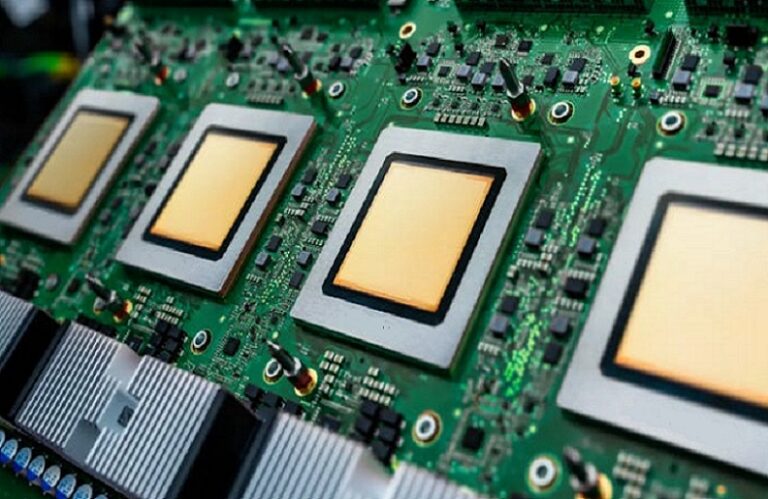
HDI PCB for GPU hardware uses high density interconnect structures, high-layer count stackups, microvias, via-in-pad, ELIC, multi-stage HDI, low-loss Megtron…