





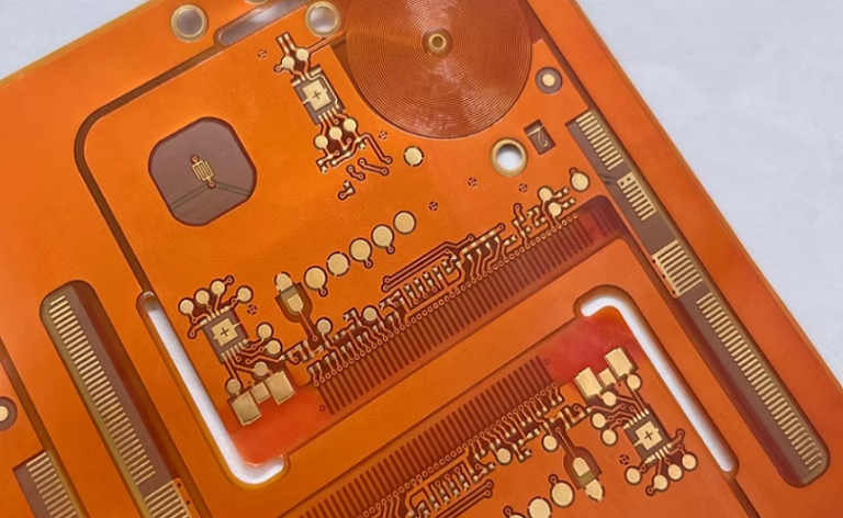
Flexible PCB Design Guidelines
Flexible PCB design succeeds when the mechanical bend, copper pattern, dielectric stack-up, coverlay, stiffeners, and component zones are engineered as…

Flexible PCB design succeeds when the mechanical bend, copper pattern, dielectric stack-up, coverlay, stiffeners, and component zones are engineered as…
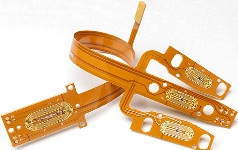
Flexible PCB manufacturing services provide advanced circuit solutions for electronic products that require lightweight structures, compact packaging, and mechanical flexibility.…
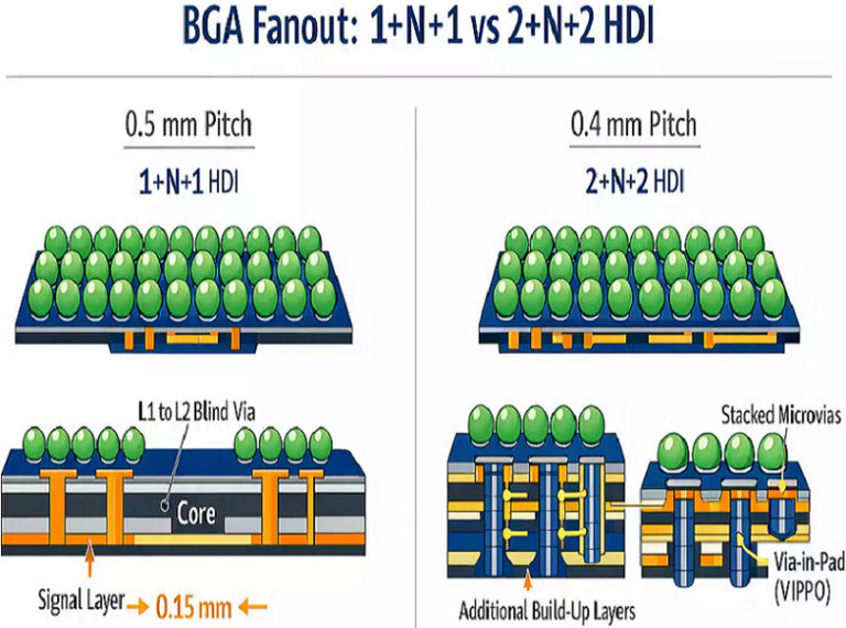
Selecting the right High-Density Interconnect (HDI) PCB supplier is critical for electronic products that require compact design, high-speed performance, and…
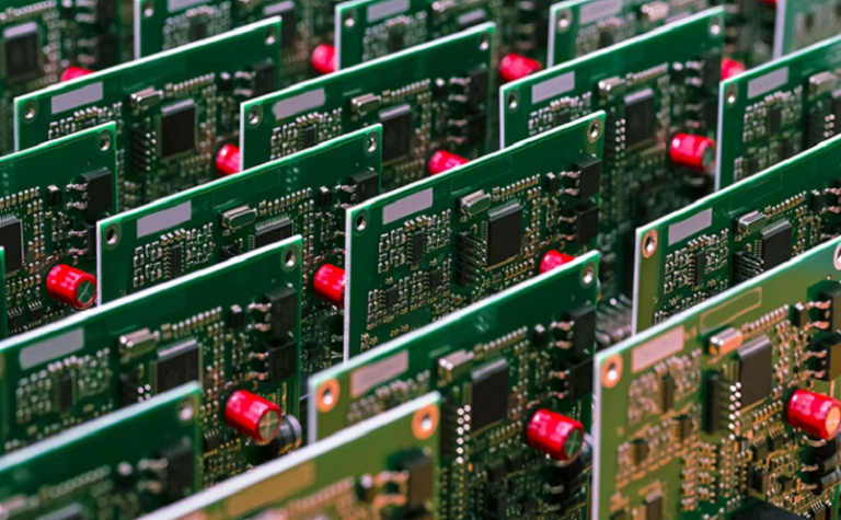
HDI PCB Assembly involves advanced manufacturing technologies that enable smaller electronic products, faster signal transmission, and improved power distribution. However,…
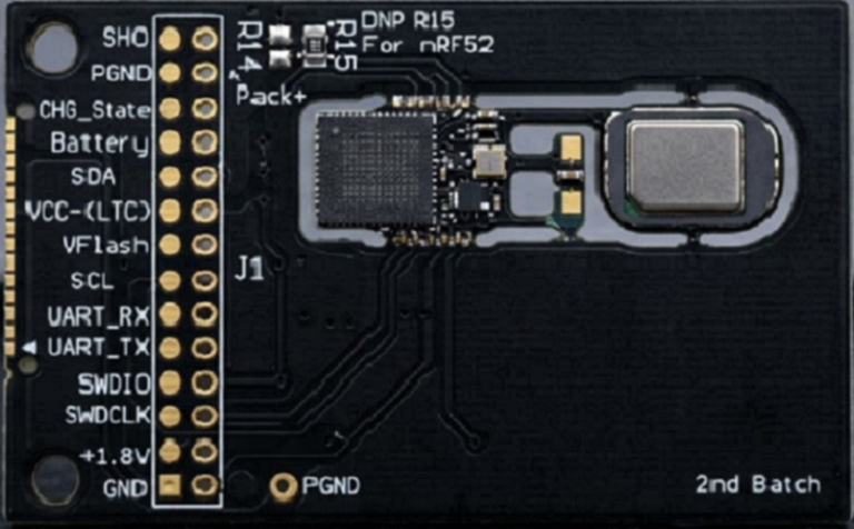
High density interconnect technology has become the preferred PCB architecture for modern IoT products because it combines miniaturization, electrical reliability,…
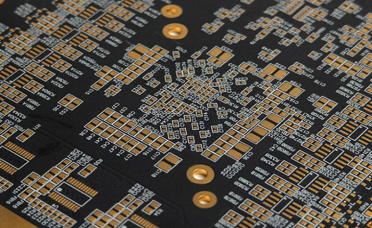
HDI PCB for automotive electronics is a high-density interconnect technology used in advanced vehicle systems such as ADAS radar modules,…
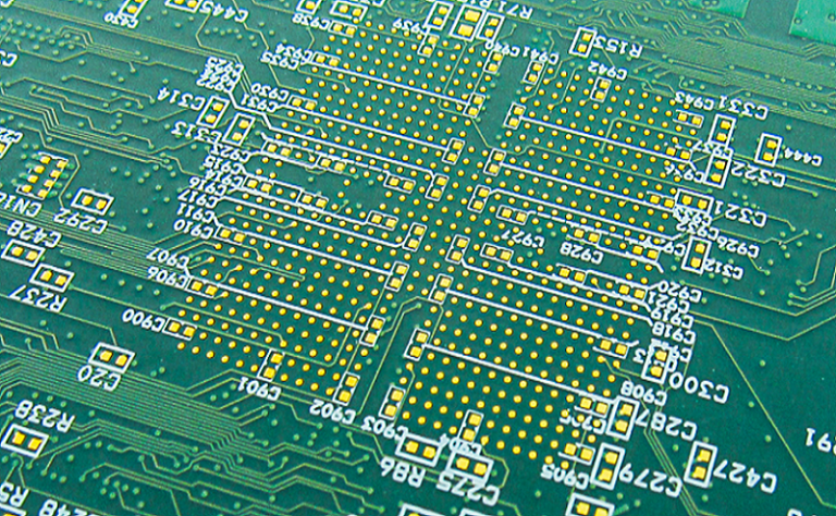
HDI PCB for medical devices is a high-density interconnect technology used in compact healthcare electronics where high reliability, signal integrity,…
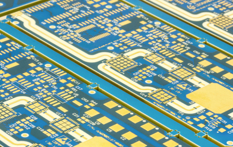
HDI PCB material selection means matching electrical loss, dielectric stability, laser drillability, thermal reliability, copper foil profile, and fabrication capability…
HDI PCB testing and quality control verify whether high density interconnect boards can meet electrical, mechanical, thermal, and reliability requirements…