Rigid Flex PCB Cost Optimization Guide
Rigid flex PCB cost is usually higher than a standard rigid PCB because it combines rigid board fabrication, flexible printed…
Rigid flex PCB cost is usually higher than a standard rigid PCB because it combines rigid board fabrication, flexible printed…
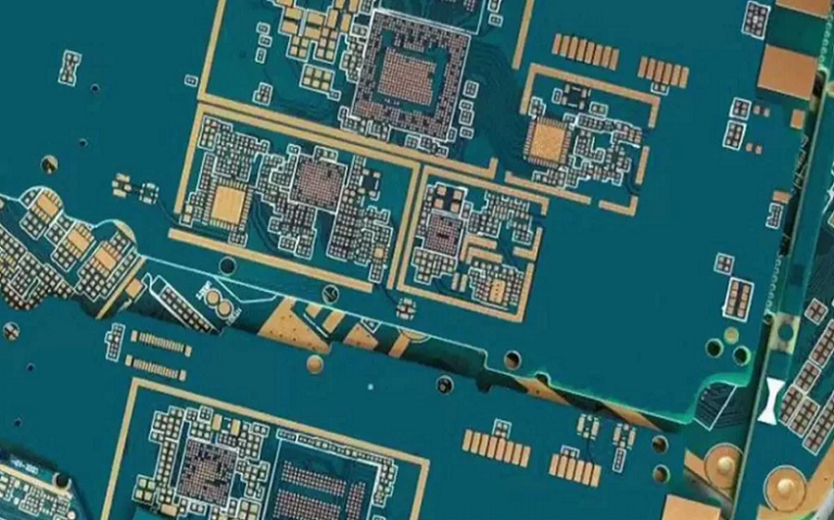
HDI PCB manufacturing builds high density interconnect circuit boards with microvias, blind and buried vias, fine line routing, sequential lamination,…
High speed rigid flex PCB design demands precise control of impedance continuity, layer stackup symmetry, flex mechanical limits and EMI…
Impedance control in rigid flex PCB ensures consistent characteristic impedance (50Ω single-ended, 100Ω differential) across rigid and flexible sections, critical…
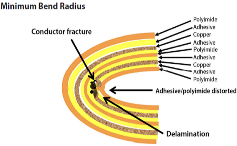
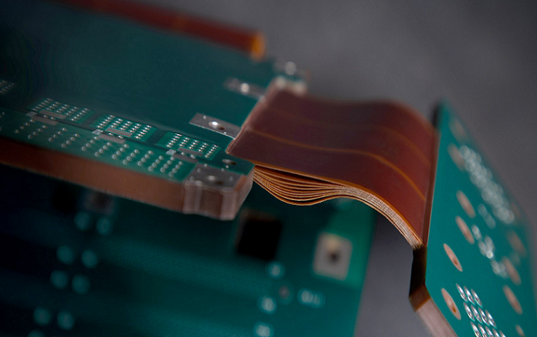
Flex bend radius is the most critical mechanical parameter in rigid flex PCB design, defining the minimum curvature a flexible…
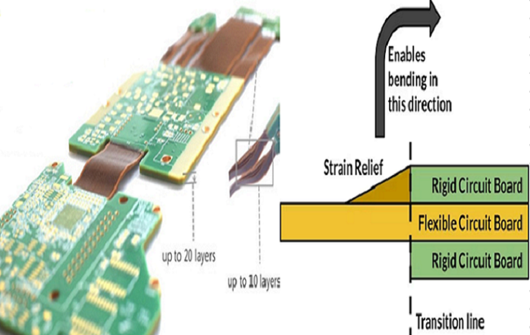
Rigid flex PCB design for manufacturing integrates mechanical bendability, electrical performance, and fabrication feasibility into a unified workflow, ensuring high…
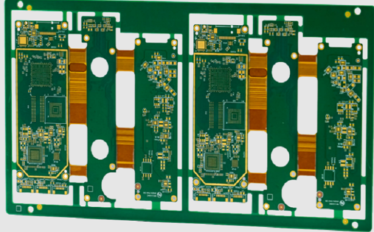
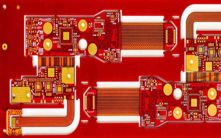
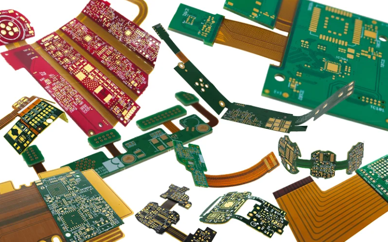
Rigid-flex PCB integrates rigid FR‑4 sections and flexible polyimide layers into a monolithic interconnection system, classified by IPC‑6013 standards and…
Built as a hybrid electronic circuit structure, rigid-flex PCB combines rigid substrate sections for component mounting and durable flexible film…
Rigid-flex PCB represents a hybrid circuit solution that integrates rigid dielectric substrates and flexible polyimide layers into a single unified…