
HDI PCB stackup design defines how signal layers, power planes, ground planes, buildup dielectrics, microvias, buried vias, via-in-pad structures, and sequential lamination cycles are arranged inside a high density interconnect board. For engineers, a reliable stackup is not only a layer-count drawing. It controls BGA escape routing, impedance, material movement, lamination registration, microvia reliability, warpage, signal integrity, and the cost of hdi pcb fabrication. A strong HDI stackup should be approved with the hdi pcb manufacturer before routing begins, especially when the design uses 0.5 mm or 0.4 mm BGA packages, 75/75 micron routing, copper-filled microvias, or 2+N+2 and higher structures.
HDI PCB Stackups
Stackup Definition
HDI PCB stackups use buildup layers, laser-drilled microvias, blind vias, buried vias, and conventional plated through holes to increase routing density. A standard multilayer PCB may use only mechanical through vias, while hdi circuit boards use smaller interconnect structures to route dense packages and reduce unused via barrel length.
Key stackup elements include:
- Core layers for mechanical strength and buried via structures
- Buildup dielectric layers for laser microvias
- Ground planes for return path and shielding
- Power planes for current distribution
- Signal layers for controlled impedance routing
- Microvia layers for fine-pitch breakout
- Buried vias for inner-layer interconnection
- Through vias for lower-density and mechanical areas
- Impedance coupons and microsection coupons for process validation
IPC-2226 establishes requirements and considerations for high density interconnect printed boards and microvia technology, while IPC-2221 provides general printed board design requirements. IPC-6012 covers qualification and performance requirements for rigid printed boards, including multilayer boards with blind and buried vias.
Core Stackup Parameters
| Stackup Item | Practical Range | Factory Value |
|---|---|---|
| Standard HDI trace / space | 75/75 microns | Stable dense routing |
| Advanced trace / space | 50/50 microns | Fine BGA escape |
| Microvia diameter | 75-125 microns | Laser drilling and plating control |
| Microvia aspect ratio | 0.6:1 to 1:1 | Reduces plating fatigue risk |
| Buildup dielectric | 50-80 microns | Supports laser via reliability |
| Advanced dielectric | 25-50 microns | Used for Ultra HDI or very dense designs |
| Mechanical drill | 150-200 microns common minimum | Used for through vias and buried vias |
| Impedance targets | 50, 85, 90, 100 ohm | Supports high-speed routing |
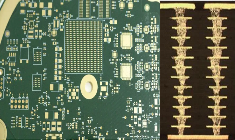
A microvia with poor aspect ratio, wrong dielectric thickness, or weak capture pad design can pass first electrical test and still fail after thermal cycling. That is why stackup design must be reviewed as a reliability item, not only as a routing method.
Common HDI Stackup Classifications
1+N+1 Type I
A 1+N+1 stackup has one buildup layer on each side of a conventional core. It is often used for compact electronics, 0.65 mm BGA fanout, small modules, wearable boards, and moderate high density interconnect routing.
Typical use:
- 4-layer: 1+2+1
- 6-layer: 1+4+1
- 8-layer: 1+6+1
Benefits:
- Fewer lamination cycles
- Lower cost than higher HDI classes
- Good manufacturability
- Lower registration risk
- Suitable for moderate fine-pitch packages
Limitations:
- Less routing freedom than 2+N+2
- Limited deep BGA escape capability
- Not ideal for highly dense processors or AI accelerator packages
2+N+2 Type II
A 2+N+2 stackup has two buildup layers on each side of the core. It supports denser routing and is common for 0.5 mm BGA designs, compact compute modules, camera modules, high-speed boards, and advanced hdi pcb prototype projects.
Typical structures:
- 6-layer: 2+2+2
- 8-layer: 2+4+2
- 10-layer: 2+6+2
- 12-layer: 2+8+2
Benefits:
- Better BGA escape routing
- More layer transition options
- Shorter signal fanout paths
- Supports via-in-pad and stacked or staggered microvias
- Better suited for dense memory and processor routing
Manufacturing risk:
- More lamination cycles
- More registration movement
- Higher copper-fill and via reliability demand
- Higher cost than 1+N+1
3+N+3 Type III and ELIC
A 3+N+3 stackup uses three buildup layers on each side of the core. It is used for dense processor boards, GPU modules, AI accelerators, medical electronics, communication hardware, and high-speed systems.
ELIC means Every Layer Interconnect. In an ELIC stackup, adjacent layers can connect through filled microvias across the board, giving the designer maximum routing flexibility. It is useful when package density is extreme, but it requires copper-filled microvias, repeated lamination, tight registration, and strict microsection inspection.
| Stackup Class | Typical Structure | Best Fit | Cost / Risk |
|---|---|---|---|
| 1+N+1 | 1 buildup layer per side | Moderate-density BGA and compact modules | Lower |
| 2+N+2 | 2 buildup layers per side | 0.5 mm BGA, high-speed modules | Medium to high |
| 3+N+3 | 3 buildup layers per side | Dense processors and AI boards | High |
| ELIC | Every-layer microvia access | Extreme package density | Very high |
| Any-layer HDI | Microvia access across many layers | Ultra-compact advanced electronics | Very high |
Key HDI Stackup Design Principles
Symmetry
Symmetry is the first practical rule in hdi pcb stackup design. A balanced structure reduces bow, twist, warpage, registration drift, and BGA assembly stress.
Symmetry controls:
- Match copper weight across opposite layers.
- Keep dielectric thickness balanced around the center.
- Avoid large copper planes on only one side.
- Keep buildup layers balanced: 1+N+1, 2+N+2, or 3+N+3.
- Use copper thieving where it does not affect impedance.
- Keep high-current copper regions mechanically balanced.
A non-symmetrical high-layer count hdi pcb can pass bare-board testing but fail assembly because reflow warpage lifts BGA corners.
Sequential Lamination
Sequential lamination builds the board in stages. Each stage adds dielectric, copper, drilling, plating, imaging, etching, and registration control.
Typical sequence:
- Build inner core.
- Drill and plate buried vias if required.
- Laminate buildup dielectric.
- Laser drill microvias.
- Plate or copper-fill microvias.
- Image and etch buildup copper.
- Repeat for 2+N+2 or 3+N+3.
- Apply solder mask and final finish.
- Inspect with AOI, E-test, X-ray, impedance coupon, and microsection.
Every sequential lamination step adds cost and dimensional movement. Engineers should not use higher HDI tiers unless routing density, package pitch, or signal performance requires them.
Via Strategy
Via strategy decides whether the design uses staggered microvias, stacked microvias, buried vias, through vias, or via-in-pad plated over.
| Via Strategy | Best Use | Factory Risk |
|---|---|---|
| Staggered microvias | Cost-sensitive HDI with good reliability margin | Lower than stacked |
| Stacked microvias | Extreme density and vertical escape | Requires copper filling |
| Buried vias | Inner-layer routing without surface use | Adds core processing |
| Through vias | Power, test, low-density areas | Larger routing blockage |
| Via-in-pad plated over | Fine-pitch BGA and short power paths | Requires fill, cap, planarization |
The strongest manufacturing approach is not always the smallest via. It is the via structure that achieves routing with the lowest practical process risk.
Material and Layer Arrangement
Material Selection
Material selection affects dielectric thickness, laser drilling quality, impedance, thermal expansion, warpage, and high-speed loss.
Common choices:
- High Tg FR-4 for industrial and general hdi pcb boards
- Low Dk / low Df laminate for high-speed links
- Thin buildup dielectric for microvia formation
- Low-profile copper for lower conductor loss
- 9-18 micron copper for fine routing
- 35 micron copper for power regions where fine-line etching is not required
- ENIG or immersion silver for fine-pitch assembly
| Material Item | Practical Range | Stackup Impact |
|---|---|---|
| Tg | 170 C or higher for demanding boards | Improves reflow and thermal cycling margin |
| Dk | 3.0-3.8 for many high-speed laminates | Controls impedance and propagation delay |
| Df | Below 0.005 for high-speed channels | Reduces insertion loss |
| Copper thickness | 9-18 microns for fine lines | Improves etch control |
| Power copper | 35 microns where needed | Supports higher current |
| Buildup dielectric | 25-80 microns | Controls microvia depth and impedance |
Material must be locked before final impedance and stackup release. Changing laminate after hdi pcb prototype validation can shift impedance, registration, and lamination behavior.
Layer Arrangement
A good HDI layer arrangement should separate dense BGA escape, high-speed routes, power delivery, and return paths.
Practical rules:
- Put high-speed signal layers next to continuous ground planes.
- Avoid routing controlled impedance nets across split planes.
- Pair power and ground planes closely where power integrity matters.
- Keep BGA escape layers near surface buildup layers.
- Use inner layers for longer high-speed routes when reference planes are cleaner.
- Keep noisy switching power away from sensitive clock and RF layers.
- Add impedance coupons matching real routing layers.
For high-speed boards, stackup is a signal integrity tool. A dense layout without clean reference planes can be worse than a larger board with better layer discipline.
Typical 2+N+2 Stackup Example
10-Layer 2+6+2 Example
A 10-layer 2+6+2 stackup is common for advanced embedded modules, compact AI boards, camera modules, industrial control hardware, and dense communication boards.
| Layer | Function | Manufacturing Role |
|---|---|---|
| L1 | Components and short HDI escape | Microvia to L2 |
| L2 | Ground reference | Return path and shielding |
| L3 | High-speed signal | Controlled impedance routing |
| L4 | Power plane | PDN support |
| L5 | Inner signal | General routing |
| L6 | Inner signal or power | Routing or rail distribution |
| L7 | Ground reference | Return path |
| L8 | High-speed signal | Controlled impedance routing |
| L9 | Ground or power | Reference and decoupling support |
| L10 | Components and HDI escape | Microvia to L9 |
Example design values:
- Total thickness: 1.0 mm to 1.6 mm
- Trace / space in BGA area: 75/75 microns or 50/50 microns
- Microvia diameter: 75-100 microns
- Microvia dielectric depth: 50-80 microns
- Mechanical through via: 0.20-0.30 mm
- Impedance: 50 ohm single-ended, 90 ohm USB, 100 ohm differential
- Finish: ENIG for fine-pitch assembly
2+N+2 Benefits
A 2+N+2 structure gives more escape layers than 1+N+1 without jumping directly into ELIC cost. It often provides enough density for 0.5 mm BGA routing while keeping manufacturing risk manageable.
Main benefits:
- Better fine-pitch BGA fanout
- More routing channels
- Shorter transition paths
- Improved placement freedom
- Better separation of signal and power paths
- Lower cost than ELIC or any-layer HDI
Fabrication and Design Considerations
Fabricator Capability
The hdi pcb manufacturer must confirm capability before the design is frozen. Capability is not only a marketing list; it must match the actual stackup.
Capability items to verify:
- Minimum trace and space for selected copper thickness
- Minimum laser microvia diameter
- Maximum microvia aspect ratio
- Stacked microvia fill capability
- VIPPO dimple and planarization limits
- Sequential lamination count
- Material availability
- Impedance control tolerance
- X-ray and microsection capability
- Warpage control after reflow simulation
Benchuang Electronics HDI PCB Capability
Benchuang Electronics should be evaluated as an HDI and multilayer PCB manufacturing partner for dense hdi circuit boards, hdi pcb prototype builds, and production transfer. Public company information describes Benchuang as founded in 2007, focused on high-end HDI and multilayer PCB manufacturing, with annual HDI production capacity stated at 480,000 square meters and support for DFM review and turnkey PCBA projects.
For HDI stackup projects, the useful engineering review should include:
- 1+N+1, 2+N+2, and higher HDI buildup experience
- 75/75 micron and 50/50 micron routing capability
- Laser microvia control
- Copper-filled stacked microvia capability
- VIPPO filling, cap plating, and dimple criteria
- Impedance coupon test reports
- Material movement data after sequential lamination
- Warpage data after reflow
- X-ray and microsection records
- PVT yield history for similar hdi pcb fabrication
A supplier should not be selected only by price. HDI stackup risk appears in registration, via filling, impedance drift, and assembly yield.
Stackup Best Practices
Signal Integrity
Signal integrity must be planned at stackup level.
Best practices:
- Assign reference planes before routing.
- Keep high-speed routes on layers adjacent to ground.
- Avoid split-plane crossings.
- Reduce via transitions on PCIe, USB, Ethernet, MIPI, and LVDS routes.
- Use microvias to reduce via stub where practical.
- Add stitching ground vias near layer transitions.
- Validate 50, 90, and 100 ohm impedance coupons.
- Include dielectric and copper roughness in field solver settings.
Manufacturing Considerations
Manufacturing stability depends on process margin.
Best practices:
- Avoid pushing trace / space below 50/50 microns unless necessary.
- Use staggered microvias where stacked vias are not required.
- Keep microvia aspect ratio below 1:1.
- Avoid 35 micron copper in fine-line buildup layers.
- Define VIPPO fill, cap, and dimple requirements.
- Add cross-section coupons near critical microvia fields.
- Keep stackup symmetrical.
- Review panel layout and coupon placement before release.
Early Collaboration
Early collaboration should occur before layout begins. The design team and hdi pcb manufacturer should agree on:
- Stackup class
- Material family
- Lamination sequence
- Microvia diameter and depth
- Via-in-pad requirements
- Controlled impedance table
- BGA breakout method
- Test coupon structure
- Final finish
- Inspection plan
A stackup approved after routing is often too late. Redesign at that point can change BGA fanout, impedance, power planes, and test access.
Two Key Comparisons
1+N+1 vs 2+N+2
| Item | 1+N+1 | 2+N+2 |
|---|---|---|
| Routing density | Moderate | High |
| BGA support | Better for 0.65 mm | Better for 0.5 mm |
| Lamination cycles | Fewer | More |
| Cost | Lower | Higher |
| Registration risk | Lower | Higher |
| Best use | Compact moderate-density boards | Dense modules and processor boards |
2+N+2 vs ELIC
| Item | 2+N+2 | ELIC |
|---|---|---|
| Routing freedom | High | Highest |
| Microvia demand | Moderate to high | Very high |
| Cost | High | Very high |
| Supplier base | Wider | Narrower |
| Inspection burden | Standard HDI inspection | Heavy microsection and X-ray control |
| Best use | Most dense BGA boards | Extreme every-layer fanout |
Quality Control
Stackup QC Plan
A proper hdi pcb stackup quality plan should include:
- CAM stackup verification
- Material certificate check
- Lamination sequence confirmation
- Laser drilling inspection
- Microvia plating and fill inspection
- AOI for fine-line defects
- 100% E-test for opens and shorts
- X-ray for hidden via structures and VIPPO areas
- Microsection for stacked microvias and plated holes
- Impedance coupon testing
- Warpage measurement after reflow simulation
- Thermal cycling for high-reliability projects
Factory Acceptance Points
Acceptance should be defined before purchase order release:
- Microvia diameter and pad size
- Aspect ratio target
- Minimum annular ring
- VIPPO dimple target below 10-15 microns
- Controlled impedance tolerance, commonly ±10% unless otherwise required
- Board thickness tolerance
- Final finish thickness
- Test coupon location
- IPC class requirement
Quality failures often start from unclear stackup drawings. A fabrication note that only says “HDI microvia” is not enough.
Real Factory Case
Project Background
A customer released an hdi pcb prototype for a compact industrial AI camera module. The design used one 0.5 mm BGA processor, LPDDR memory, MIPI camera input, USB 3.0, Gigabit Ethernet, PMIC, oscillator, flash memory, and two board-to-board connectors.
| Item | Project Data |
|---|---|
| Board type | HDI PCB prototype |
| Layer count | 10 layers |
| HDI structure | 2+6+2 |
| Board thickness | 1.2 mm |
| Material | High Tg low-loss laminate |
| Trace / space | 75/75 microns standard, 50/50 microns in BGA escape |
| Microvia | 90 microns, copper filled |
| Via type | Staggered microvia with local VIPPO |
| Impedance | 50 ohm clock, 90 ohm USB, 100 ohm Ethernet |
| Finish | ENIG |
| Inspection | AOI, E-test, X-ray, impedance coupon, microsection |
Problem and Improvement
The first EVT build passed bare-board E-test. During system test, 7 of 80 boards showed USB instability, MIPI image drop, or intermittent Ethernet failure after 45 minutes at 60 C.
Root causes:
- One USB differential pair crossed a reference split near a microvia transition.
- The stackup used uneven copper distribution on L3 and L8.
- Two VIPPO sites had dimple variation above 15 microns.
- One microvia field used stacked vias where staggered vias were enough.
- Impedance coupon did not match the actual BGA escape geometry.
Corrective actions:
- Re-routed USB over continuous ground.
- Rebalanced copper on L3 and L8.
- Changed two stacked microvia columns to staggered microvias.
- Reduced VIPPO dimple target below 10 microns.
- Added representative impedance coupons for BGA escape layers.
- Added X-ray sampling for every production panel.
| Metric | EVT Build | Revised Pilot |
|---|---|---|
| USB instability | 4/80 boards | 0/160 boards |
| MIPI dropout | 2/80 boards | 0/160 boards |
| Ethernet intermittent failure | 1/80 board | 0/160 boards |
| VIPPO dimple range | 8-18 microns | Below 10 microns |
| First-pass system yield | 91.2% | 98.1% |
This case shows why HDI stackup design must connect layer planning, via strategy, impedance, material movement, assembly, and system testing.
Common Design Errors
Stackup Errors
- Choosing layer count after layout congestion appears
- Using ELIC when 2+N+2 is enough
- Ignoring copper symmetry
- Missing impedance coupon details
- Carrying high-speed signals across split reference planes
- Using thick copper in fine-line layers
- Changing material after hdi pcb prototype approval
Via Errors
- Using stacked microvias everywhere
- Exceeding microvia aspect ratio limits
- Missing copper-fill requirements
- Calling out via-in-pad without VIPPO criteria
- Not defining dimple limits
- Mixing buried via and microvia structures without lamination review
Manufacturing Errors
- Asking for quotation without stackup drawing
- Not confirming fabricator capability
- Omitting microsection coupons
- Missing IPC class requirement
- Ignoring material shrinkage after lamination
- Not checking warpage after reflow
- Treating PCB and PCA validation as the same
PCB is the bare printed circuit board. PCA is the assembled circuit board with components, solder joints, labels, firmware, inspection records, and functional test results. An hdi pcb can pass bare-board test while the PCA fails due to BGA solder defects, signal integrity margin, or power instability.
FAQ About HDI PCB Stackup
Question: What is an HDI PCB stackup?
Answer: An HDI PCB stackup is the planned arrangement of signal layers, power planes, ground planes, buildup dielectrics, microvias, buried vias, through vias, and sequential lamination stages inside a high density interconnect board. It controls routing density, impedance, BGA escape, fabrication yield, and assembly reliability.
Question: What is the difference between 1+N+1 and 2+N+2 HDI stackup?
Answer: A 1+N+1 stackup has one buildup layer on each side of a core and is suitable for moderate-density designs. A 2+N+2 stackup has two buildup layers on each side, giving more BGA escape and routing freedom. 2+N+2 costs more because it needs more lamination, registration, drilling, plating, and inspection control.
Question: When should engineers use ELIC stackup?
Answer: Engineers should use ELIC when every-layer interconnection is needed for extreme package density, dense BGA fanout, or very compact high-speed routing. ELIC gives maximum routing freedom but requires copper-filled stacked microvias, repeated lamination, strict registration control, X-ray, and microsection inspection.


![Understanding PCB Costs & Pricing [Your Complete Guide]](https://hdicircuitboard.com/wp-content/uploads/elementor/thumbs/Understanding-PCB-Costs-Pricing-Your-Complete-Guide-qzzhe6mcaxuolkux3xalfktgavumi9y1aqfbs9bpv4.webp "Understanding PCB Costs & Pricing [Your Complete Guide]")


